 robert.c.baruch
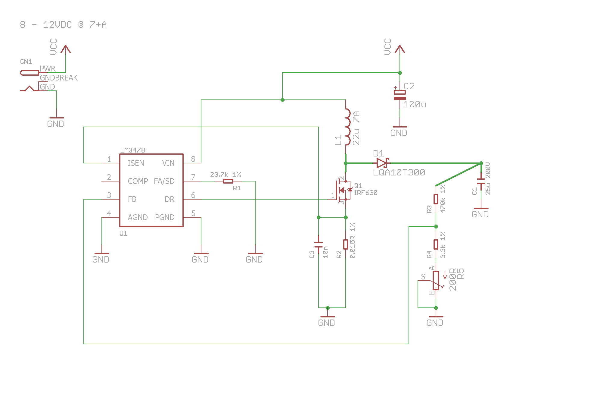
Goal: Design a boost converter that gives 170VDC at 0.15A from a 12VDC supply.
Adafruit has a nice boost converter calculator, assuming you're using the simple single-inductor version. To power my boost converter, I'd like to use a 12VDC wall adapter. I don't know, but suspect that the output voltage of the adapter will drop under load, so I'm just going to go ahead and specify a minimum input voltage of 8VDC. Min and max output voltage are 170VDC, output current is 0.15A, I'll specify an output ripple voltage of 2V, and a switching frequency of 150kHz. I hate low-frequency converters with their whining. Shut up already, converter!
This gives me a required inductance of at least 17.5uH capable of handling 4.25A. Also a duty cycle (switch on-time to total time) of 0.953. This rules out the popular MC36033, which has a max duty cycle of 0.857.
TL;DR: After the design procedure, here's what I ended up with:
Design procedure
The LM3478 datasheet provides a nice series of design procedures for various converter topologies. Here's the one for the boost converter:
Switching frequency
First, choose a switching frequency between 100kHz and 1MHz. I chose 150kHz because I wanted it to be above the minimum, but not so fast that all my components had to be super-fast.
Duty cycle
Next, compute the duty cycle, D. We got this from the Adafruit calculator, 0.953. Also convenient is the inverse duty cycle (proportion of off-time to total period), D' = 1 - D.
Note that the converter will adjust the duty cycle based on the output voltage and switch current, so this is only a value for calculation.
Minimum inductance
Compute the minimum inductance required. Again, this is from the Adafruit calculator, but here is the formula:
So with a maximum input voltage of 12V, and an output current of 0.15A, I get L > 12uH. Note that the Adafruit calculator (correctly, in my opinion) uses the lowest of two possible duty cycle based on the minimum input and output voltage, because this will result in the highest minimum inductance. In any case, I chose L = 22uH as a convenient value.
Maximum inductor current
Compute the maximum current flowing through the inductor. Again, Adafruit gives this as 4.25A, but the formula is:
And so I get a current of 4.92A. Again, Adafruit correctly is using the D based on the maximum input voltage, but I'm using a higher value for extra safety margin.
So based on the inductance and current, I can choose an inductor that can handle this current. Thus, I chose the Bourns 2105-H-RC, capable of 7A.
Frequency adjust resistor
The LM3478 uses this formula:
With my chosen frequency of 150kHz, I get 135.4k. I chose a 133k 1% resistor which slightly increase the frequency to 152kHz. I'll keep using 150kHz in the calculations as it doesn't matter much.
Current sense resistors
One of these is the resistor that goes between the switch and ground. This resistor protects the circuit against overload currents. We use the maximum inductor current from above, plus an additional 20% margin, to set the overload threshold:
And so I get a sense resistor of 0.014 ohms. I chose a standard resistor of 0.015 ohms (Stackpole BR3FB15L0). With that resistor, the current limit would be 5.52A, well within the maximum required 4.92A and the 7A spec for the inductor.
There is a second resistor which goes between the current sense pin of the converter and the current sense resistor. The datasheet recommends adding this resistor when the duty cycle is above 50% to prevent sub-harmonic oscillations (that is, oscillations lower than the switching frequency) caused by instability in the loop. No whiny converters!
We first calculate the maximum sense resistor for current mode loop stability (loop stability is always a good thing):
I get a maximum sense resistance of 0.004 ohms. Our chosen sense resistor is bigger than this by a factor of 3.75, so we need to add that second "slope compensation" resistor:
This yields 6.325k as the minimum slope compensation resistor.
The problem is that addition of this resistor modifies the current limit:
We must now change both the sense resistor and the slope compensation resistor so that the current limit is sane and the slope compensation resistor is above the minimum. Doing so (without going through the math) shows that it is not possible to pick a reasonable sense resistor while still maintaining a good current limit.
The cause of this is the insanely low maximum sense resistance from above. There are two ways to raise that maximum sense resistance: raise the frequency, or raise the inductance. Doing that also has a knock-on effect of lowering the inductor current. So this is really a good thing.
Thus, instead of a maximum sense resistance of 0.004 ohms, let's get this above 0.015 ohms so we can use the nice current sense resistor I found. This means raising the frequency (or the inductance) by at least a factor of 3.75. Since I kinda like the inductor I chose, let's raise the frequency from 150kHz to 600kHz and try again.
Our modified values with this frequency are:
The new current limit, of course, didn't change from before because we chose the same sense resistor. However, we now do not need a slope compensation resistor, and everyone is happy.
Diode selection
The diode has to be able to carry the maximum inductor current. It must also be able to withstand a reverse bias of the output voltage minus the input voltage. And, a Schottky diode is recommended for high speed. I chose the Power Integrations LQA10T300 diode, which has a max reverse bias of 300V and a current limit of 10A. The datasheet also says it is capable of 1A/ns, so presumably it can turn off a current of 3.62A in 3.62ns.
MOSFET selection
Look at the frequency, and then the duty cycle. The off-time is 0.047 / 600kHz = 78ns.
The LM3478 datasheet, however, kind of gives up on being able to choose a MOSFET. Other than being able to withstand the output voltage at the drain (max Vds) and the inductor current (max Id) and being able to turn the MOSFET on in the first place (threshold Vgs < 7.2V), the only real recommendations are for a low on-resistance and for it to be "fast". Clearly such a switch has to shut off well before 78ns.
I chose the STMicro IRF630 MOSFET. It can withstand at least 200V to the drain, and has a gate threshold of at most 4V. It can handle currents up to 9A, and has an on-resistance of 0.35 ohms.
Can this thing switch fast enough? Nobody will know unless we try it. If not, there are chips specifically designed to drive MOSFET gates at higher currents to force them on and off quickly.
Output capacitor selection
You want something big with low ESR. I chose the Panasonic EZP-E50256LTA, 25uF, 500V, ESR of 8.8 mohm.
Compensation
There's a COMP pin on the converter where you put a resistor and capacitor in series. They are there to add stability to the converter. The converter is a feedback loop, and such feedback loops need to be stable, otherwise your power supply might fail at certain frequencies. We will be following Application Note 1286, Compensation for the LM3478 Boost Converter. If you don't know anything about control theory, you probably want to skip this section. The problem is, without knowing control theory, it will be difficult to select the compensation components. Maybe start with this list of videos?
So, let's take a look at the application note to see what the transfer function looks like without this compensation.
We see that there are two zeros, one pole, and one complex pole:
The first zero, z1, is caused by the output capacitor with its ESR. The second zero, z2, is caused by the inductor and the load on the power supply. The pole is caused by the output capacitor with the load, and the complex pole is caused by the switching action.
Let's locate the zeros:
From this, we have (I'll show frequencies in Hz rather than rad/s):
Note that the second zero is a right-hand plane zero. This means that in gain it acts like a zero, but in phase it acts like a pole.
Next, we locate the simple pole as follows:
And so:
And now for the complex pole. We need to find Q, which is the damping factor. If Q were infinite, the thing would vibrate itself to pieces and catch fire at half the switching frequency. But, of course, this will not be the case.
Remembering that VSL = 92mV from the datasheet, we have:
And, of course, this pole is located at half the switching frequency:
Now that we have our pole and zero frequencies, we need to know what the DC gain is. It is:
where VFB is the feedback threshold voltage, 1.26V from the datasheet. So, we have:
OK, at this point I could draw a Bode plot by hand, but I have Mathematica, so I'll just leave this here:
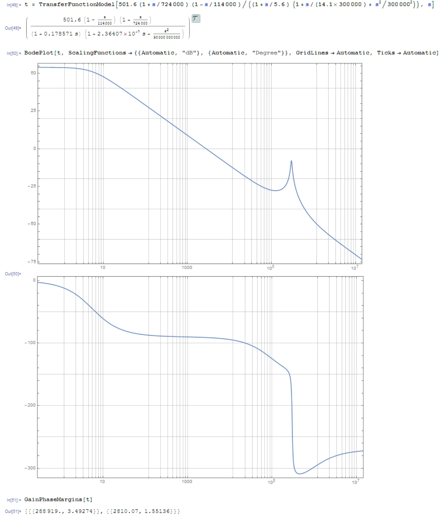
The top plot is gain in dB vs frequency in Hz, and the bottom is phase shift in degrees vs frequency in Hz. You can see the resonance at half the switching frequency.
The phase margin is 180 degrees plus the phase at which the gain is unity (0 dB). We can see that unity gain occurs at 2.81 kHz and the phase margin there is 1.551 radians (88.9 degrees). This is fine, since the application note states we want a phase margin between 30 and 100 degrees.
The gain margin is minus the gain at which the phase is -180 degrees. Here we see the gain margin is 3.5 = 10.9 dB at 289 kHz.
These margins are important because the poles and zeros shift with varying load and input voltage, and without these margins your circuit could go unstable. However, the margins cannot be too great otherwise the system doesn't react quickly to changes.
The datasheet doesn't state this, but ideally the gain margin should be somewhere between 6 and 12 dB. And indeed it is.
So, in fact, this converter with the components so far needs no compensation network, and we can leave the COMP pin unconnected.
Conclusion
Well actually there is no conclusion until I actually get the parts in to build this thing. Will it work? We'll find out in the next project log.
Discussions
Become a Hackaday.io Member
Create an account to leave a comment. Already have an account? Log In.
I was thinking of using this chip in a 5V nixie power supply. I even simulated it in LTSpice. Then I started reading about the compensation circuit and realized that I don't have the means to calculate it. Even the duty cycle calculation is problematic - I am planning to use a transformer, the feedback is driven from the secondary, but the chip is driving the primary. In fact, I am not even sure what value I would insert into the equations for the impedance in the case of a transformer. That is all before you get to the need to plot charts to solve the equations. I think I will have to look at other chips such as the LT1619.
Anyway, this is a good worked example, and very relevant!
Are you sure? yes | no