 Chuck Glasser
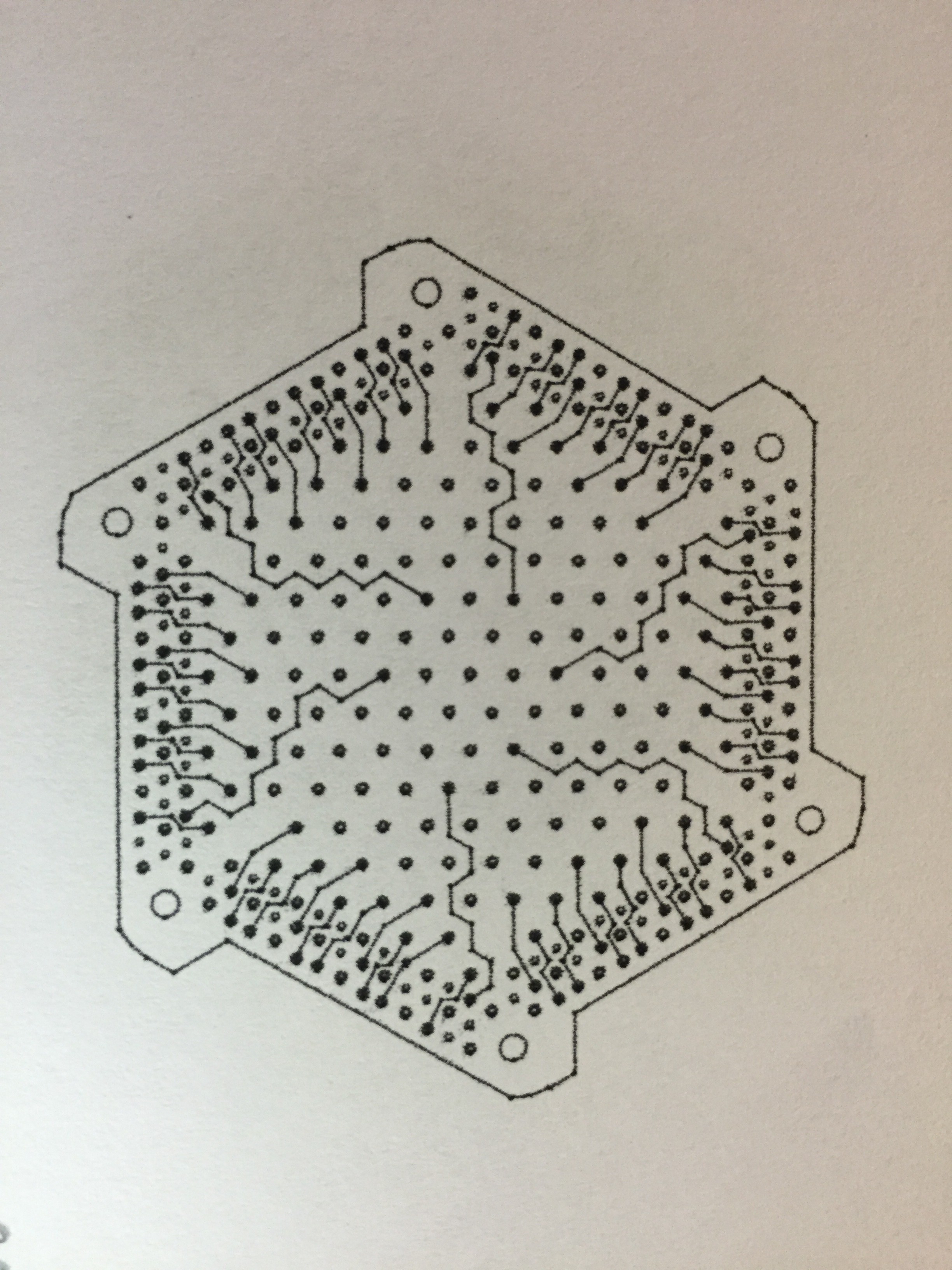
So the essential detail in building a system that can produce working circuits with 3 mil design rules is keeping all the various processes registered. That means that if a hole is laser drilled at X = 3.455685, Y = 5.343366, and later come back to via fill that hole, the fill operation is at the same coordinate, and so on.
That means that any artwork needs to be made in such a way that lines of ink end up the same way. Always located at a precise location corresponding to all the other precise locations. In other words, all the various processes have the same reference point.
What this means is that even though the ink jet printer may not be used to print silver ink, it serves very well as part of the mask making process for the screen printer.
To review, there are only 6 operations in making a LTCC circuit.
Blanking, via filling, circuit printing, stacking, pressing, and firing.
For blanking either a CO2 or 455nm laser may be used, or a drag knife, and/or a hot drag knife. For minimal residue, a knife seems best. For holes, pulsed laser.
For vias and lines we'll use a screen.
The screens will be made by first printing a registered transparency onto the vacuum table. The Ink jet is used to print the pattern.
A registered screen is then place on top of the transparency and the artwork is exposed from below or more practically, simply removing the transparency and registering it to the screen frame.
The key is that everything is registered to a set of pins on the CNC table. Tape, artwork, screen printing frame, laser, camera, cutters, etc.
In this case the 6 holes at each of the hexagon apexes will be used.
Discussions
Become a Hackaday.io Member
Create an account to leave a comment. Already have an account? Log In.