 Chuck Glasser
Just a few days ago I awoke with the thought that I needed to check Ebay for bargins: It didn't take long to find it.
One of the realities of dealing with all ceramics is that they shrink when fired. That is especially critical when there are many layers with carefully placed traces and vias interconnecting the various layers.
In general there are three methods to control shrinkage. Each method tries to minimize shrinkage in the X and Y axis and confine material changes to the Z axis.
Heraeus, HL2000 "zero shrink" tape is made up of uniformly sized grains of material say 8 to 12 microns. This methods gives a shrink factor of much less than 1% in the X & Y whereas the Z may change by %20, whereas one might expect to find 15% in X & Y with ordinary tape in which the particles are whatever came out of the ball mill. The second method is constrained sintering in which the green tape is glued to an alumina substrate and fired. Electro Science Laboratories provides materials for this method. The third method places a weight upon the surface of the tape while it is fired. That is what this pressing furnace is designed for.
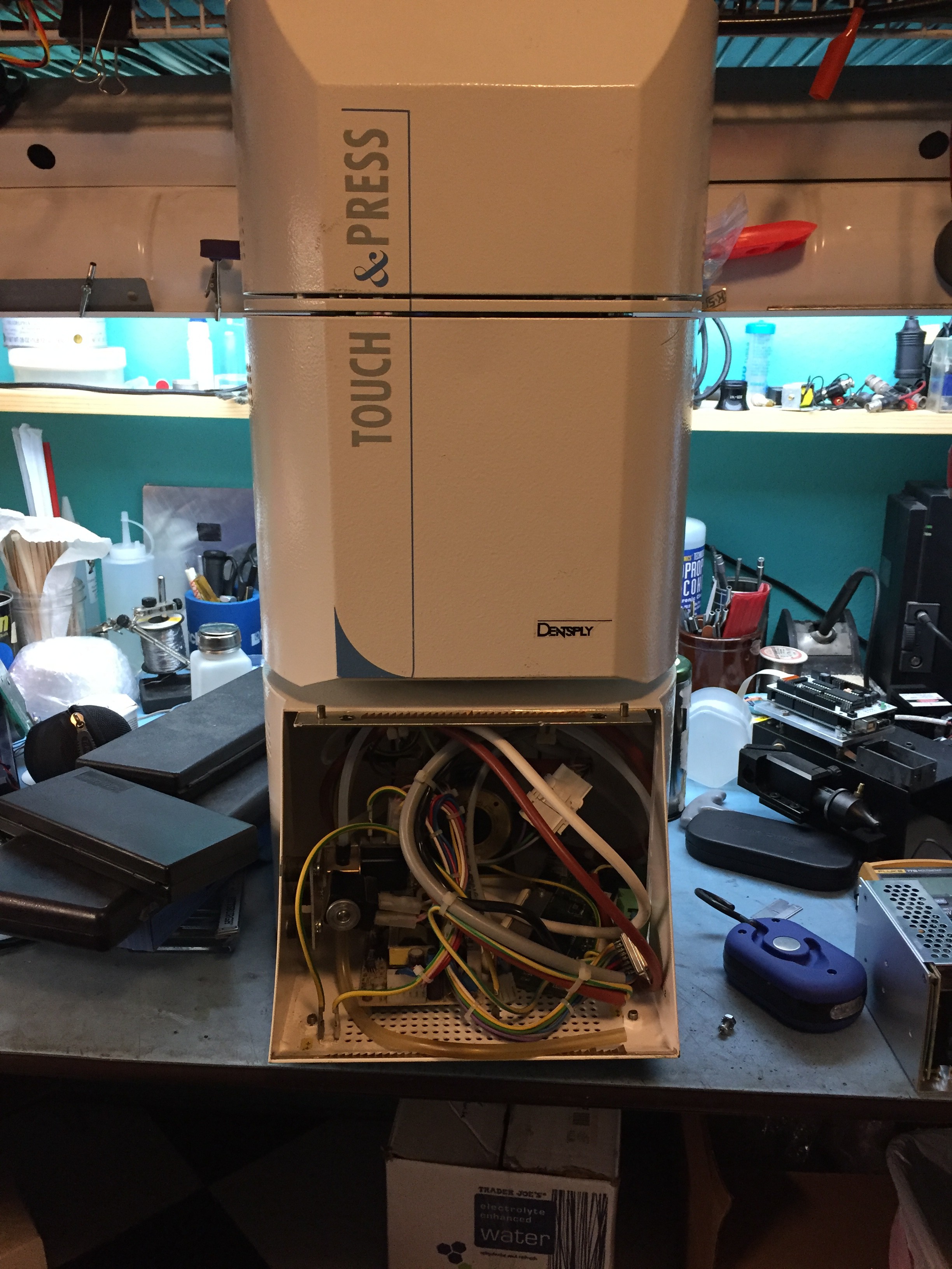
You can probably guess why it was such a great bargin! No matter. An ATMega or Beaglebone Black, display, a few relays and sensors should make it right in no time.
Discussions
Become a Hackaday.io Member
Create an account to leave a comment. Already have an account? Log In.