 Ted Yapo
I haven't posted a log on this project for a while. Since last time, this project was selected as a semi-finalist in the Hackaday Prize 2016. I was really blown away to see this. Seriously, this project consumed my thoughts and my life for a long time, and it's awesome to have it recognized in this way. Thanks to all the decision makers for their consideration!
Substituting Components
There are a few component substitutions I need to test. First, the original inductors on the DDL01 boards are no longer in production - in fact, no inductors in that package seem not to be made in 2016! I found some possible replacements, but before I re-spin the tightly-packed board, I figured I should test them out with the existing PCB. I had to order some more boards for this. and they're arriving tomorrow, so it's time to prepare for the tests.
The second substitutions are for the 1N4007 diodes. RF PIN diode switching is an "off-label" usage for the 1N4007, marketed as a rectifier diode, so the performance isn't guaranteed by the manufacturers' specifications. The first ones I tested worked, and I stuck with that manufacturer (Fairchild). I now have samples of 1N4007's from all the manufacturers I could find, and I'm going to see if they perform just as well (or better) than the original parts.
Finally, I'm going to test substitutions for the ferrite cores used in the DDL02 power supply. I remember being intimidated by the prospect of winding magnetics like this when I first started with RF circuits, and would like to run some quantitative tests to show that the inductors and cores used here aren't particularly critical (apart from getting the wires connected correctly). Hopefully, I can allay any apprehension prospective builders might have about these components and the power supplies.
I'll have to wait for the DDL01 boards to arrive to test the new components, but I can outline the testing methodology and run some baselines with the original components in the interim.
DDL01 Testing
I came up with a few ways to test the performance of the DDL01 gates. Here's a brief overview:
Eye Diagrams
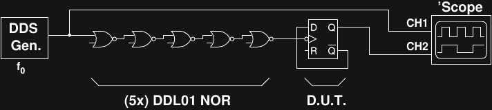
The first test is designed to examine the performance of a single DDL gate. One of the difficulties in this test is creating a "DDL" input waveform to drive the device-under-test. Around the lab I have either 50-ohm signal generators or 5V CMOS outputs, neither of which is a good approximation of a DDL output. My solution is to use a chain of DDL01 inverters to condition the signal before input to the D.U.T. Of course, now you're testing the whole chain, but major differences in performance of the D.U.T. due to component substitutions should be detectable.
Here's the test circuit. I use a DDS generator to make an accurately adjustable clock driving the CLKin pin on a PIC 16F723A. I had a handful of "breakout boards" made for this part since I've used it in a few projects and have a partial tube of them left over. The PIC is programmed with a simple 9-bit linear feedback shift register producing a 512-bit pseudo-random bit stream. The inner loop of the assembly code is 12 cycles long; combined with the CLK/4 oscillator divider, this results in a 1/48 clock division. Not great for high-speed work, but perfectly adequate here. One of the PORTB pins outputs the pseudo-noise sequence while another outputs a synchronized clock for triggering the scope.

In case anyone's interested, here's the simple PIC assembly. It uses the carry bit in the status register as part of the 9-bit shift register since the RRF instruction rotates through the carry - an easy way to double the length of the sequence without introducing more instructions.
;;;
;;; PIC16F723A LFSR pseudo-random bitstream generator
;;;  using 9-bit LFSR (regsiter + carry bit)
;;;   with polynomial x^9 + x^5 + 1
;;;
    LIST        P=16F723A
#include    <p16f723a.inc>
    errorlevel -305			;suppress warnings about default file dest
    errorlevel -302			;suppress warnings about operand not in bank 0
    errorlevel -227     ;suppress warnings about RETLW 0 instead of RETURN
    __CONFIG    _CONFIG1, _FOSC_EC & _WDTE_OFF & _PWRTE_OFF & _MCLRE_ON &_CP_OFF & _BOREN_OFF & _BORV_19 & _PLLEN_OFF
    __CONFIG    _CONFIG2, _VCAPEN_RA5
    #define   FEEDBACK_MASK  0x10
    cblock 020
      shift_register
    endc
    ORG     0
RESET:
    BANKSEL TRISB
    movlw   b'00000000'         ; set PORTB to all outputs
    movwf   TRISB
    BANKSEL ANSELB              ; make PORTB digital
    clrf    ANSELB
    BANKSEL PORTB
    movlw   0xff                ; LFSR initial state
    movwf   shift_register
MAIN_LOOP:
    movf    shift_register, W
    andlw   0x1f
    nop
    movwf   PORTB
    movlw   FEEDBACK_MASK
    btfsc   STATUS, C
    xorwf   shift_register
    rrf     shift_register
    movlw   0x20
    iorwf   PORTB
    goto    MAIN_LOOP
    END
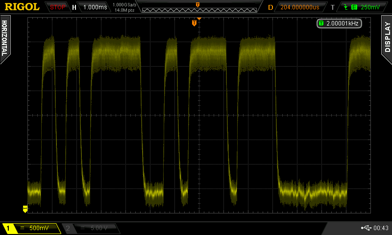
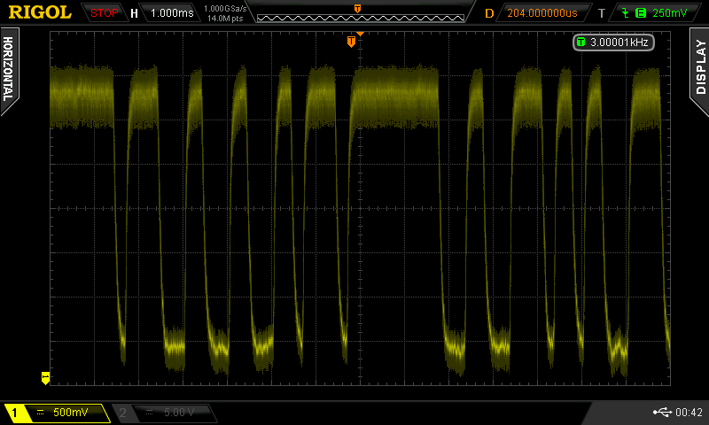
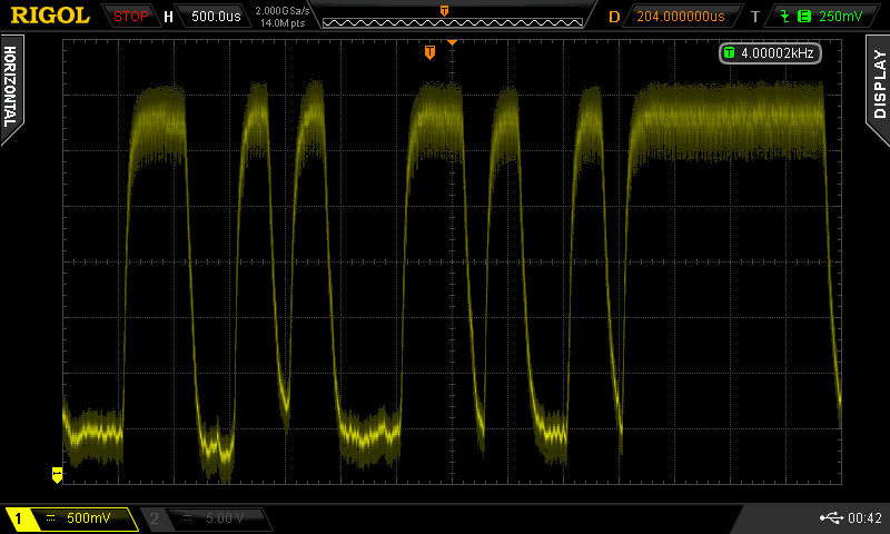
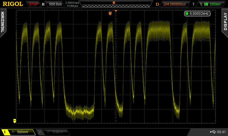
The schematic shows a DDL standard load (470 ohms plus a 1N4148 and 1N4007) attached at the output, but I omitted that load for the following tests. Here's what the eye diagram looks like at various frequencies. I changed the timescale with frequency to keep the eye size relatively constant:
 1 kHz
1 kHz
 2 kHz
2 kHz
 3 kHz
3 kHz
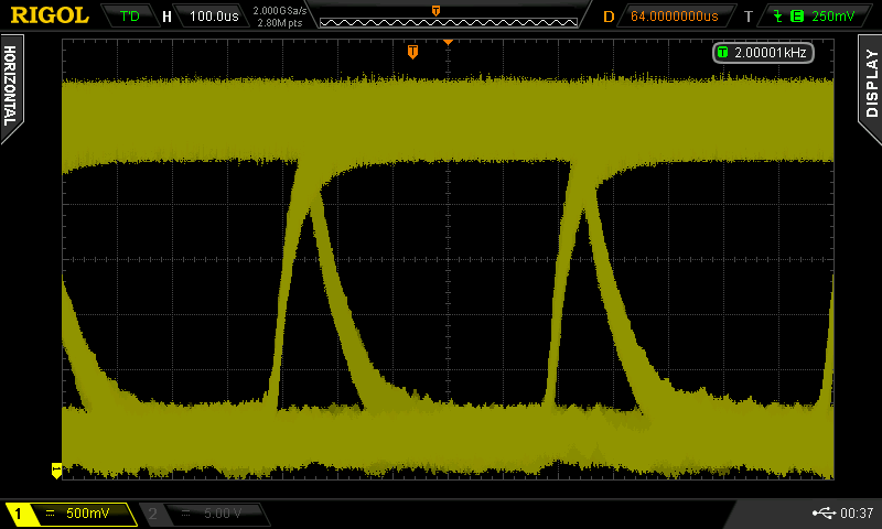
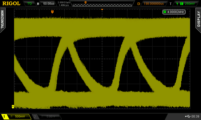 4 kHz
4 kHz
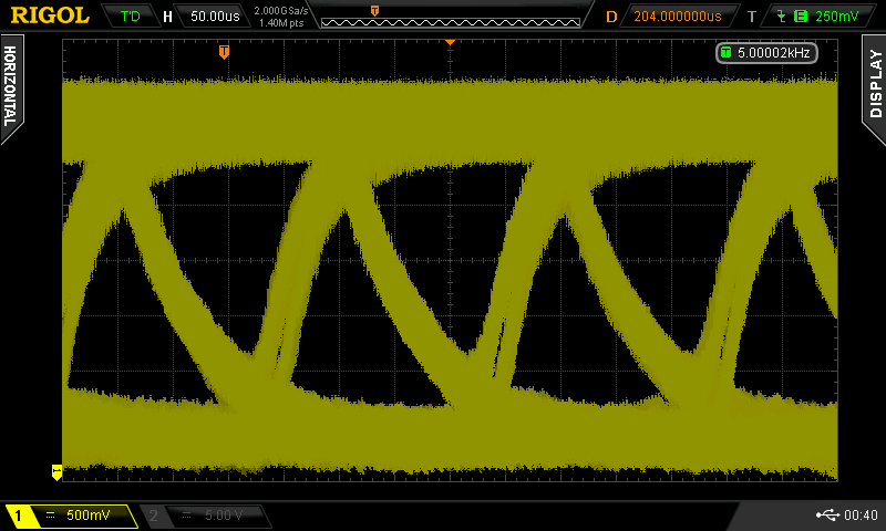 5 kHz
5 kHz
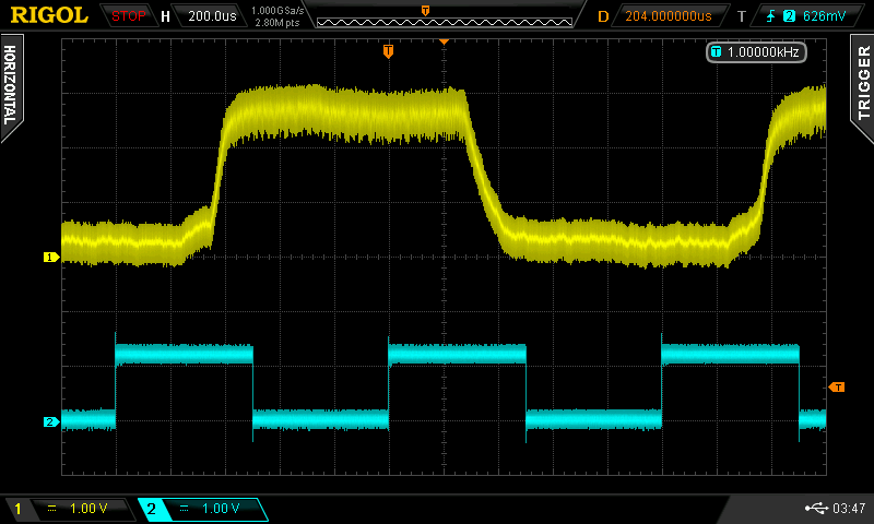
Unfortunately, because of the pure-noise power supply, the waveforms have a pretty good chance of ending up anywhere in a thick band around high or low levels. This prevents the intensity grading on the scope from producing the nice eye diagrams you may be used to seeing. With care, these are usable, though. Up to 3 kHz, the eye looks pretty good. By 4 kHz, it's getting a little tight, and by 5, some of the negative-going edges no longer make it to the bottom.
To get a better feel for the results, I also looked at the self-triggered PN bitstream:
 1 kHz
1 kHz
 2 kHz
2 kHz
 3 kHz
3 kHz
 4 kHz
4 kHz
 5 kHz
5 kHz
You can really see where there's just not enough time for the negative-edges to fall at 4 and 5 kHz. Adding extra loads to the output actually increases the speed by accelerating these edges.
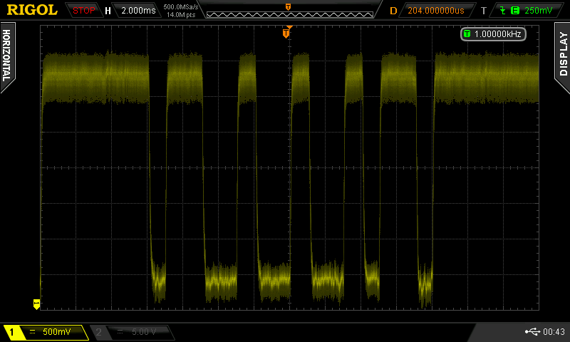
Flip-flop Toggle Speed
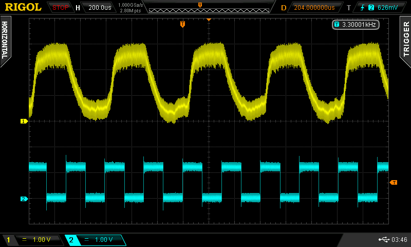
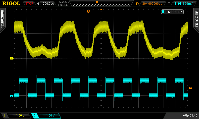
The second test I can use to evaluate new components in DDL boards examines how fast we can toggle a flip-flop. As shown in the schematic, the D-flop is wired to divide the incoming clock by two.
Triggering is awkward with this setup. Ideally you'd trigger on the DDS output, but then the phase of the flip-flop output is random, and you end up with a kind of eye diagram. If I had another DDS channel free, I could set that to half the f0 frequency and trigger on that, or I guess I could wire up a 74x74 to divide the clock for synch. By adjusting the scope holdoff, I was able to capture the following without too much difficulty:
 1 kHz
1 kHz
 2 kHz
2 kHz
 3 kHz
3 kHz
 3.3 kHz
 3.6 kHz
These measurements are in good agreement with my earlier and less organized results that ended up in the datasheet. The flip-flop reliably divides the input frequency up to about 3.3 kHz (which I listed as "typical"). 3.4 is also OK, but by 3.5, occasional glitches are noticeable. By 3.6 kHz, the output routinely drops pulses as shown.
Ring Oscillators
In an amazing coincidence, just last night I saw a very interesting log entry appear in my feed: Testing Propagation Delay. AlanX has been testing his discrete TTL circuits using inverter-ring oscillators on #A Discrete Transistor 7400 NAND GATE. I had never thought about doing this with DDL gates - so upon reading his post, I ran down to the lab and tried it - and it worked! Here's the test circuit I used:
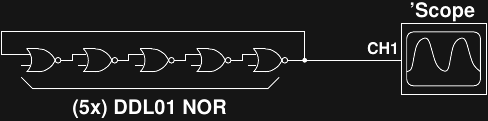
The five NOR gates are connected as before, but this time, the output is connected back to the input, closing the feedback loop, and causing the circuit to oscillate. The beauty of this circuit is that it completely eliminates the input-driver issue: signals at the "input" of this circuit appear to originate from an infinite chain of inverters! Here's what the output looks like:
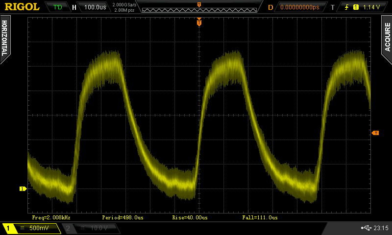
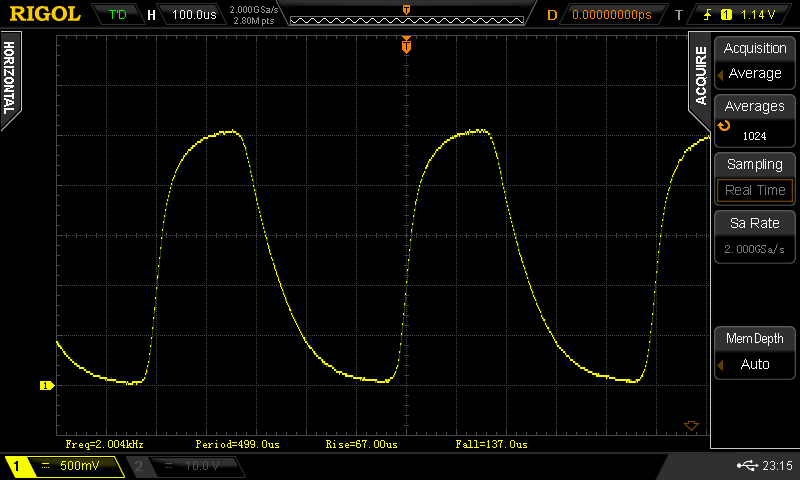
The left image uses the"sample" acquisition mode, and shows the power supply noise, as expected. On the right, the signal is averaged over 1024 samples, and provides a clean waveform for measurements. The measured frequency is 2.004 kHz (period 499 us). Assuming the H->L and L->H propagation delays are identical, this yields a 499/10 = 49.9us tpd. This is in line with the "typical" values I originally listed in the datasheet (from other measurements), but this method is much easier. The rise time of the pulses is 67us, and the fall 137us (the difference being due to the single-ended output driver of DDL gates). In total, this test gives three more data points to compare with the new components.
Next Up
The new batch of boards are arriving tomorrow, so once I populate them with the candidate components, I can run these tests and see how the substitutes perform.
Having some organized, quantitative metrics on gate performance will also allow me to revisit the design decisions involved in choosing the frequency and spectrum spreading for the power supply.
Discussions
Become a Hackaday.io Member
Create an account to leave a comment. Already have an account? Log In.