 Ted Yapo
I added an introductory video to the project details. No particularly new information, but you can see the thing run through 24 hours in a matter of seconds. Nice for fans of das blinkenlights.
Design of DDL Gates
Just for reference, here are the traditional diode gate circuits:
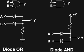
These work fine for a small number of stages, but these are the only gates they can form.
Single-Stage DDL
The first real attempt I made at a usable diode logic family, DDL 1.x, used single-stage NOR gates, like this schematic:
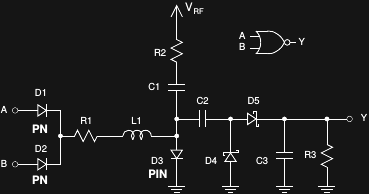
More details about this circuit can be found in the DDL Backgrounder pdf, although I know it's not the clearest technical writing. It's a diode-OR gate, a shunt PIN-diode switch and an output voltage doubler. I think if you built single-stage gates like this with an actual PIN diode at D3 and Schottky's at D4 and D5 as shown in this diagram, you might have a chance at a scalable system. Once I got it into my head that I was going to use more common diodes (purely for gratuitous shock value), I had to abandon single-stage designs. This set me back at least a year. The problem is that single-stage gates with 1N4007/1N4148 just don't have the current drive / fan-out to create large systems. I was able to get simple D flip-flops to work, and even a Johnson counter, but I couldn't easily cascade counters - there simply wasn't enough gain in the devices.
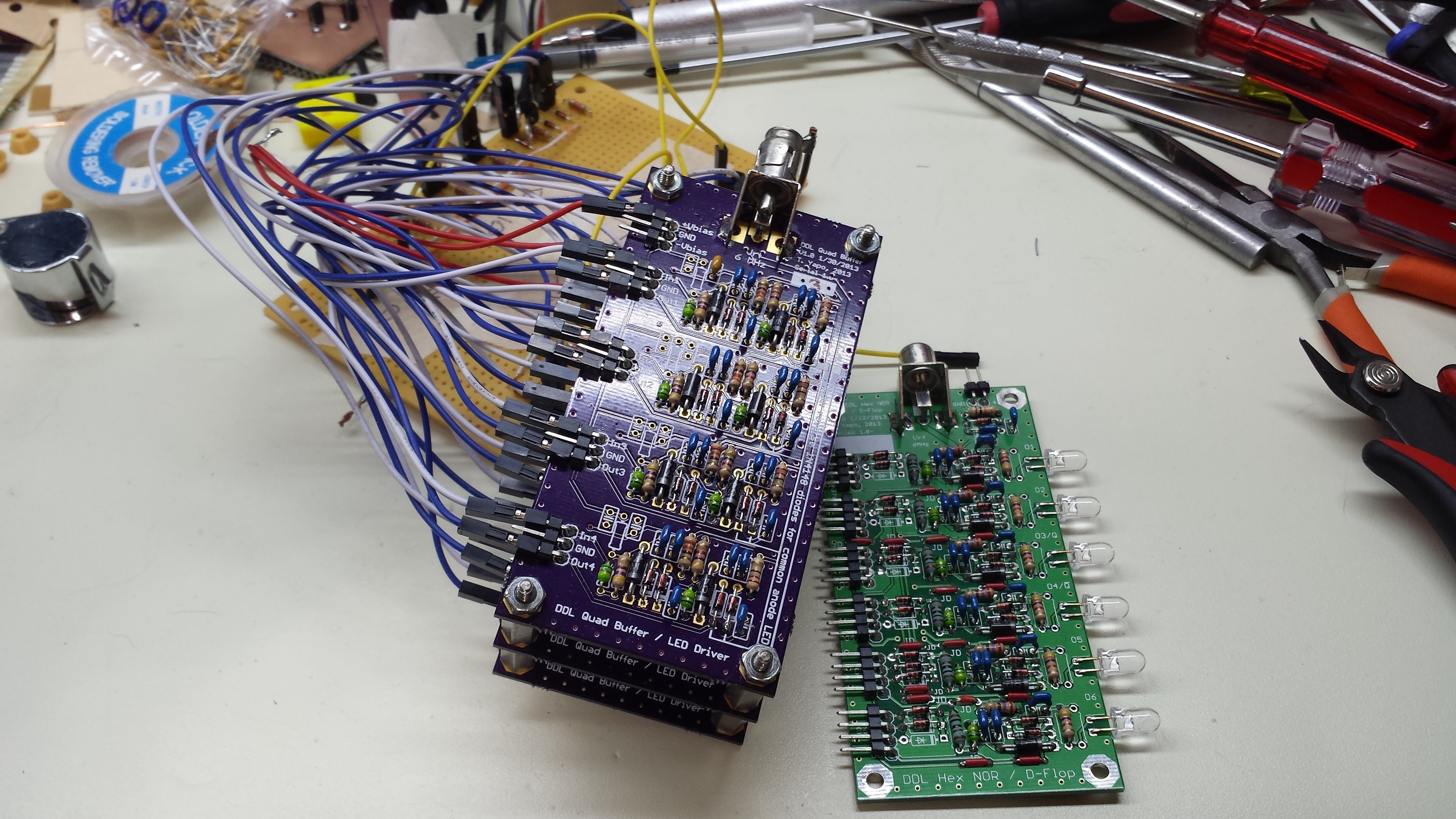
Even early on, I knew I needed two-stage gate to drive the display segments to reasonable brightness. Here's a pic of the first two-stage PCBs - the purple boards are quad two-stage drivers, while the green one is a single-stage hex NOR. This "stack" is wired as a mod-4 Johnson counter, using the 12 gates as two D-flops. It was this prototype that convinced me I needed two stages everywhere - it's been wired like this in the junk box ever since. I really did like the form factor of the single-stage boards. At 2x4", they were much more compact, quicker to assemble, and cheaper (!) than the latter generation.
Two-Stage DDL
The topology of two-stage DDL gates are explained fairly well in the datasheet, but I can't resist hitting the highlights here. Each of the six gates on the DDL01 board look like this:
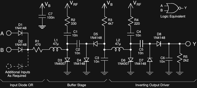
Omitted from this diagram are the front-panel LEDs and dropping resistors (640nm red and 470 Ohm from Y to ground).
The key to good current drive from the output stage is getting D6 to turn off completely. The problem is that 1N4007's have a fairly large capacitance (the datasheet says 15pF at 4V reverse bias; I measure a better figure of 15pF at 0V), plus, they're lousy PIN diodes. By applying negative bias to D6, the off-state impedance is greatly improved, allowing much more power through the output voltage doubler (C5, D7, D8, and C6). This kind of negative bias is universal practice in "normal" RF PIN diode switches. In this circuit, the voltage doubler (D4 and D5) on the first stage is reversed, so it outputs a negative voltage, overcoming the positive bias through R3.
You might think you could just use a negative bias at VB to keep D6 off. The problem is that when D4 and D5 are wired as a positive doubler, they clamp any negative bias through R3 to two diode drops, or about -1.4V, which simply isn't enough to turn D6 completely off. In the negative doubler configuration above, D6 holds its own positive bias to 0.7V, so D4 and D5 don't interfere.
It took me way too long to figure that one out.
D Flip-Flop
The driving force behind the decision to put six gates on a package was being able to make an edge-triggered flip flop, shown here:
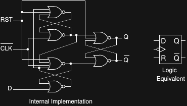
By populating the right input diodes and jumpers on the DDL01, all these connections can be done on the board, and it can just be treated as a flip-flop. It makes great counters and shift registers, and seems like just the thing for program counters or register files. Think of it as a "DDL74" (you can wire in a "Set" input as well with a few more diodes, but it's not on the current board rev., so it has to be wired externally).
I have to acknowledge Ken Bigelow's play-hookey.com site here. I had seen edge-triggered D flip-flops made from NANDs before, but after about a half hour trying to design my own NOR version, I found his (NOR D-Flop @ play-hookey.com) diagram, and based my design on that one. Thanks, Ken!
Of course, I could have just DeMorganized and reduced the NAND version, but the internet is much faster than I am.
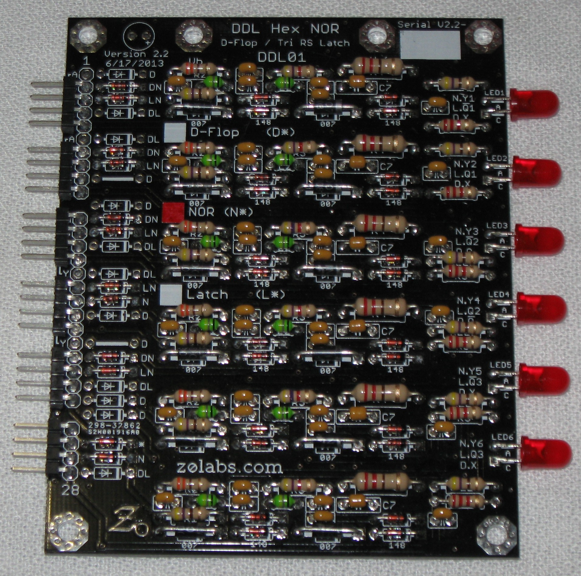
Design Files
This is what the DDL01 looks like (in basic black):
If you want one (or 46), you can either:
If you'd rather just simulate the board, here's an LTspice simulation file for a single gate from the DDL01. As with all things SPICE, take the results with a grain of salt (pun intended). I only found the simulations really useful when I couldn't be at the bench for some reason, but they're fun to play with.
The files are licensed CC-BY-SA.
Discussions
Become a Hackaday.io Member
Create an account to leave a comment. Already have an account? Log In.