 Ted Yapo
I decided to split the DDL02 documentation into multiple parts because I want to get something out there, but have to fix up some of the material before I post it all. When I developed the board, I wasn't very good about consistent part designations between the simulation, the "publication" schematic, and the board design files. It might confuse somebody (everybody?), so I'm fixing it all first. The board layout, of course doesn't need to change.
I used aluminum organic polymer caps on the DDL02 for their very low ESR, high allowed ripple current, good high-frequency response, and long life. Unfortunately, the original parts I used are now a factory special-order, so I'm in the process of finding suitable replacements. The good news is that there are now a wider variety of parts available (cheaper, too), but these are specialized caps, and it's not just a matter of finding one that physically fits on the board. A full BOM and assembly guide will be forthcoming shortly, but not in this post. Assembly of the power supply board is significantly more complex than the logic boards (which are essentially bulletproof), and it's important to get right (or risk popping MOSFETs).
Power Supply Requirements
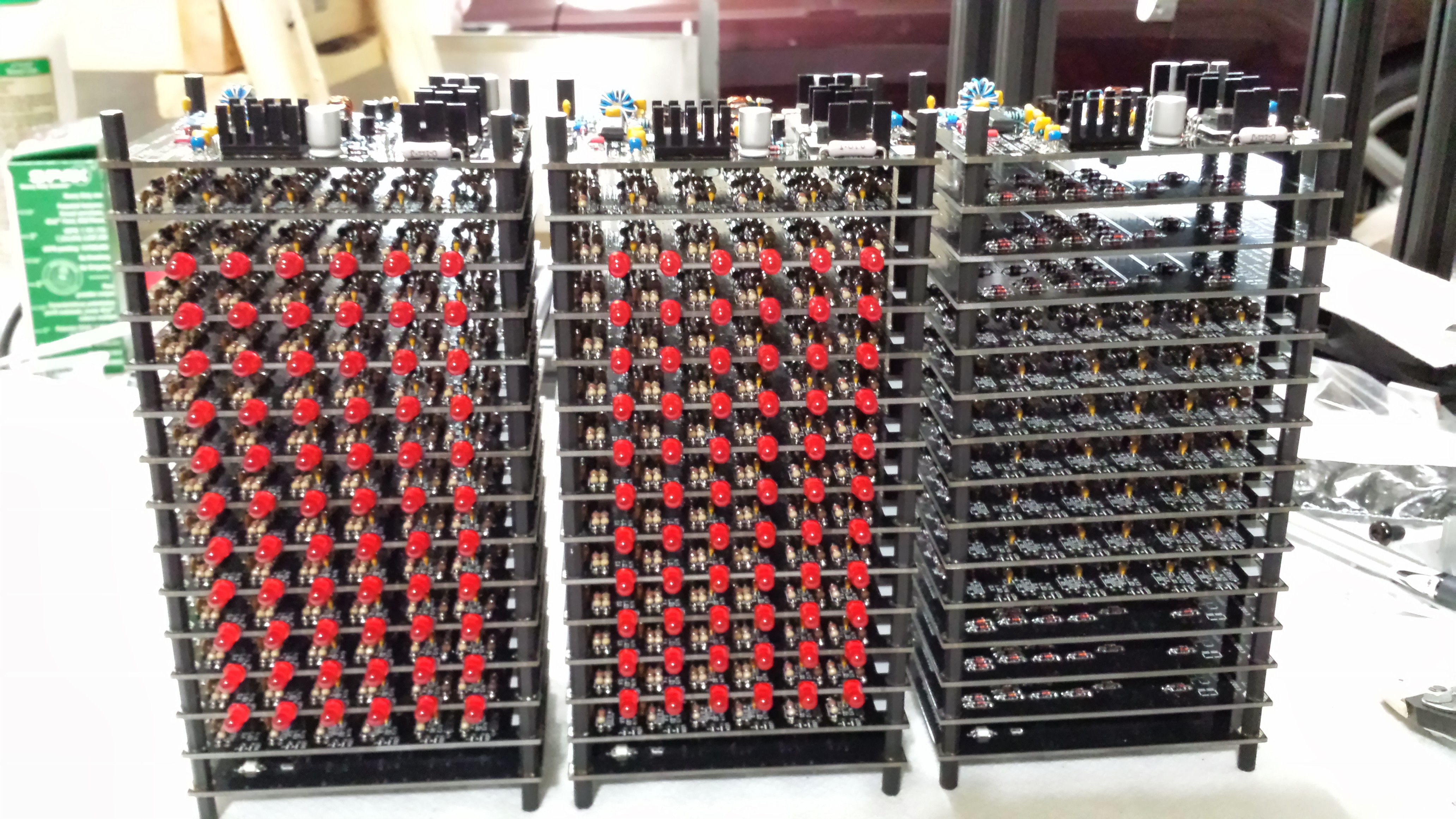
The DDL02 power supply is designed to be mounted on the left side of a DDL logic stack. Here, you can see three of the four stacks used in the clock, each with their respective power supply board mounted on "top" (these stacks are rotated 90 degrees CCW before mounting).
Here's one of the board itself:
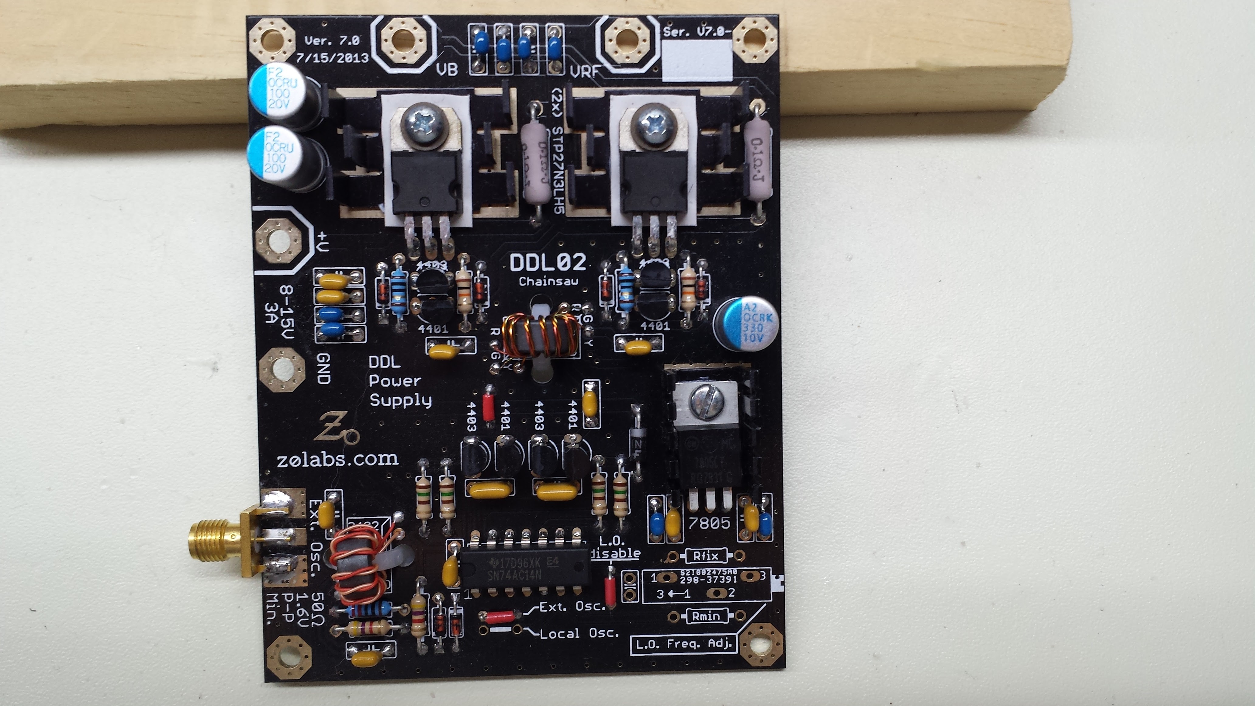
DDL requires a fairly specialized power supply, with 5V DC bias and low-impedance RF available. The 5V supply is similar to countless others - a simple 7805 drops the 12V down to 5, and a liberal sprinkling of bypass caps keeps noise at bay.
The RF supply is a different matter entirely. The DDL01 NOR board functions well with an RF supply of between 10-12 V peak-peak, and the power supply is expected to deliver that to between 1 and 20 boards per "stack". Most RF systems you'll encounter use impedance matching, in which the load impedance is matched to the source and/or transmission line impedance (typically 50 or 75 ohms). This is done to maximize power transfer as well as prevent reflections and standing waves on structures a significant fraction of a wavelength in size. Unfortunately, implementing impedance matching in a DDL system designed for modularity isn't very practical. Instead, impedance "bridging" is used, in which the source impedance is low compared to the load (similar to audio amplifiers). The DDL02 presents a source impedance of around 130 milliohms, while the expected maximum loading (20 DDL01 boards) is around 1.1 ohm. This is all at frequencies between about 1 and 10 MHz. It's not your usual HF amplifier.
History
Just for fun, this is the "Evolution of Man" chart for the DDL power supply. Except here, they're all monkeys :-)
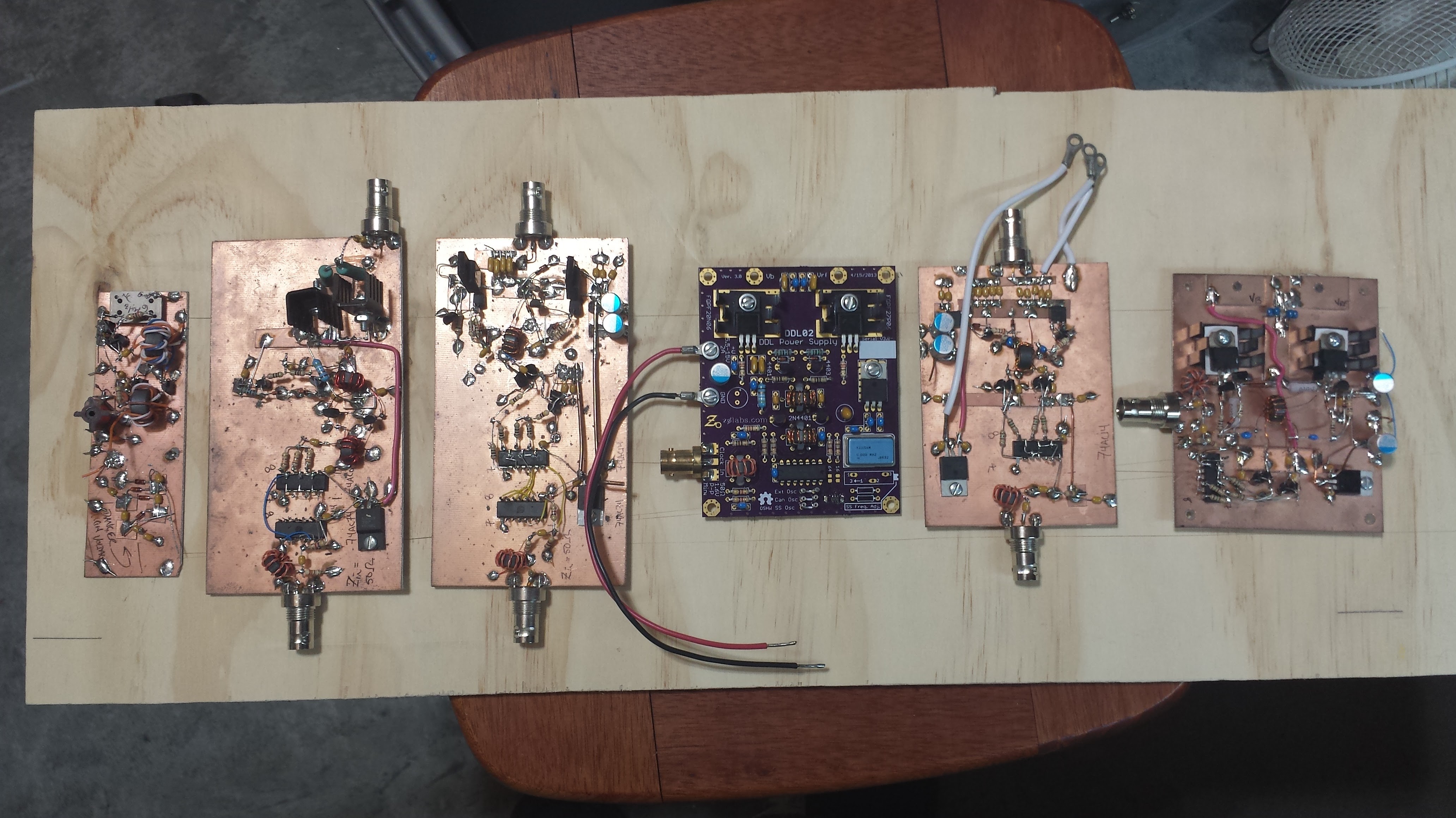
The last one on the right is essentially the same as the final PCB, and even has the correct holes and contacts for mounting on a DDL stack:
I started with complementary bipolar output devices (it's a half-bridge output driver on all but the first board), moved to complementary MOSFETs, then finally settled on two high-performance N-channel devices. Before this project, I was a little hesitant to design MOSFETs into my circuits - who needs a part that you can destroy at a touch (or, through the magic of induced charge, at the wave of a hand)? Contrast this with the humble diode, used universally as an ESD protection device. I got over it.
Design
My go-to resource for designing the supply was "Design and Application Guide for High Speed MOSFET Gate Drive Circuits" by Laszlo Balogh. You can download it here - this an external link, so if it disappears, just search for the title. I can't recommend this paper enough - if you're designing a high-speed driver with discrete components, read this paper first. Beginning to end. It will save you a lot of time.
Before I designed this circuit, I looked for suitable integrated MOSFET half-bridges and/or drivers, but could find none that offered the combination of speed and power required. However, I wouldn't be surprised if such a thing exists. If you find one, let me know.
The schematic looks like this. Click here for a nicer pdf version.
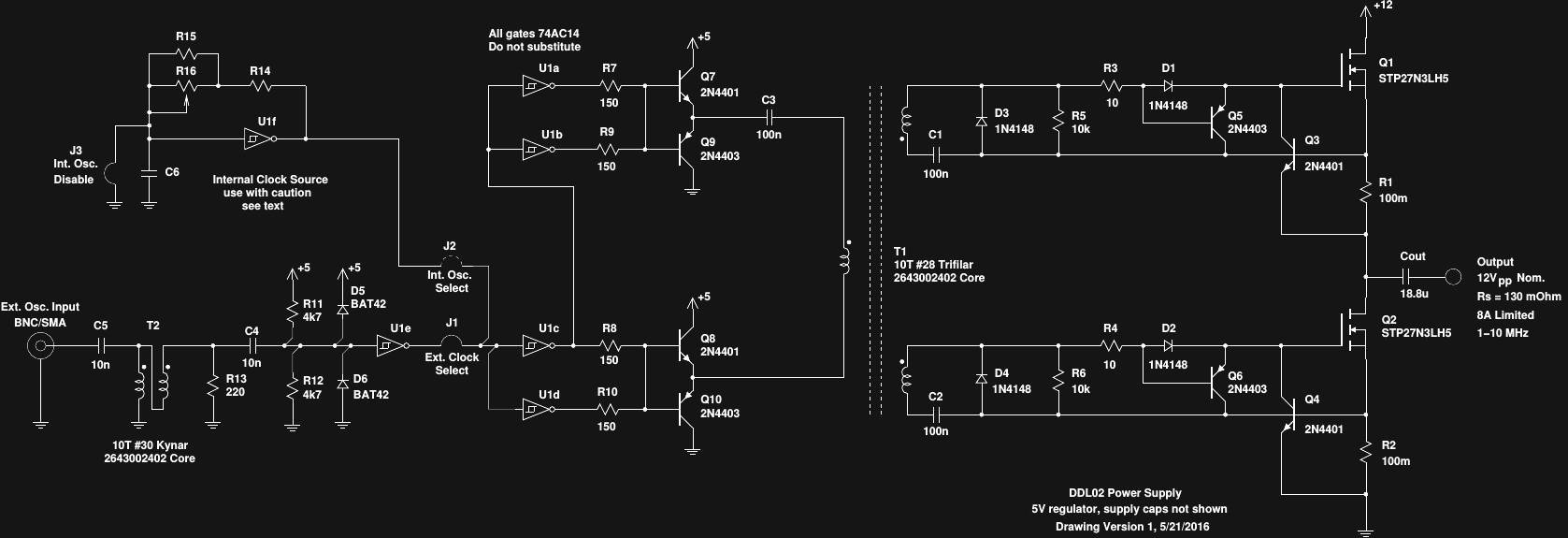
Starting with the output devices, you can see that the the high and low-side drivers are identical, and driven out of phase by two opposing transformer windings. If you build one, take careful note of the transformer phasing dots. Ignoring current-limiting for the moment, the output devices are theoretically capable of shorting over 90 Amps through each other if both turned on at the same time. Just don't do it.
The output devices used on the boards are STP27N3LH5 power MOSFETs from ST Microelectronics. A close substitute would be the PSMN022-30PL by NXP Semiconductors. I actually developed the LTspice simulation using the NXP part, because the SPICE model is readily available (see below for simulation details), but used the improved-spec ST part on the boards.
Since the high- and low-side driver circuits are identical, we'll concentrate on Q1 first. R1 and Q3 form a simple current limiter. Note the lower-case "m" - R1 is 100 milliohm, or 0.1 ohm, not 100 megaohm. When more than around 0.7V is dropped across R1, Q3 cuts off the gate drive to Q1, limiting the output current. In practice, and at the operating frequency, this limits current to about 8A peak. The result is a simple but fairly crude limiting. During limiting, the "extra" voltage, and hence power, is dropped across Q1, causing excessive dissipation. This circuit is intended to protect against momentary shorts (like accidentally grounding the output with the tip of a screwdriver), not prolonged overloads. Running this circuit in current-limiting will fry the MOSFETs eventually. The output also rings pretty badly when in limiting. Again, try not to do this.
Q5 and D1 form a "local" turn-off circuit, turning off Q1 much faster than waiting for the gate to discharge back through the transformer. To maximize the effectiveness, these parts are as close as possible to the MOSFET, keeping the gate discharge current loop small. Balogh provides a good description of this technique. While Q5 speeds the turn-off, R3 is intentionally chosen to work with the gate capacitance to slow down the turn-on. Since the high and low-side drivers are continuously alternating drive, it's important to keep them from overlapping their on-time. Even a brief overlap would mean considerable shoot-through, decreasing efficiency and increasing noise at the very least. With the design value (R3=10 ohms), I could not detect any shoot-through spikes when testing current through MOSFETs with an improvised ferrite-ring current probe. The simulation waveforms are similarly clean.
R5 serves as a power-up protection device, keeping the gate voltage low at turn-on. C1 and D3 serve to restore the DC level on the transformer secondary, clamping the negative excursions to one diode drop below Q3's source and ensuring an adequate positive gate drive voltage. Again, Balogh provides good insight.
Transformer T1 provides 180-degree phased drive to the high-side and low-side drivers. The transformer is easily wound, with some caveats. My transformers were wound on my favorite HF core, the Fair-Rite 2643002402. Mouser sells them for $0.061 (qty 100), and it works very well for broadband transformer applications like this one. The windings were done with 28-gague magnet wire, twisted together with a hand drill, then wound 10 turns on the core. I used three different colors of wire to keep the windings straight. Mixing up phasing on one of the secondaries would cause both output MOSFETs to turn on simultaneously, with disastrous results.
I will be evaluating some alternative cores on the board to verify that they work properly, and determine if they require different winding.
On the primary side of the transformer, C3 blocks DC to keep excessive current from flowing when the board is not driven (e.g. at startup or during bench testing), and eliminate any chance of DC magnetizing current from asymmetrical drive waveforms. The transistors Q7-Q10 form an H-bridge with emitter followers to dive the transformer primary in push-pull, doubling the available amplitude from the 5V supply. The transistors, in turn, are driven from paralleled 74AC14 gates (U1a-U1d). The AC-series logic drives enough current for this task; HC or TTL would not.
The clock to drive the 74AC14 push-pull stage is jumper-selected from an on-board RC relaxation oscillator or an external input. I have never used the on-board oscillator option. It was intended for small stand-alone DDL systems where the expense or complexity of the spread spectrum source was prohibitive. I also hesitate to use this source because, as a narrow-bandwidth (albeit not particularly stable) signal, it has more potential to cause interference than the spread-spectrum source. Should you decide to use it, use either R14 and R16 for a variable frequency oscillator, or just R15 (and shunt R14 with 0 ohms).
The DDL04 spread spectrum source is connected to the board through an end-launch SMA or BNC connector (builder's choice, the board will fit either). For testing purposes, a normal signal generator can be connected as well. TTL-level signals will work, as well as general 50-ohm signal generators of at least +7dBm output. The input has a reasonably good match to 50-ohms. T1 matches this to 200 ohms on the secondary, which is terminated by R11-R13. I wound this transformer with a bifilar pair made from 30 gauge wire-wrap wire because the pair has approximately 100 ohms impedance, ideal for matching 50 to 200 in a broadband transformer. In practice, a 28ga bifilar magnet wire winding (closer to 50 ohms impedance) would probably work just as well here. R11 and R12 bias U1e at mid-supply, while D5 and D6 provide protection against ESD at the input. On prototype versions of the board, I used 1N4148s here, but finally decided on the Schottkys for the production boards.
Simulation
I've uploaded an LTspice simulation for the power supply here. Since I don't have a SPICE model for the STP27N3LH5 MOSFET, I used a very similar part, the NXP PSMN022-30PL for simulations. The two parts are very similar, and probably interchangeable in this design, but I haven't tested the NXP device on actual boards. Unfortunately, even though a SPICE model is available, I can't make heads or tails of the licensing, so if you want to use it, you can download it yourself from NXP here: PSMN022-30PL SPICE model. The simulation as I supply it uses the Fairchild FDS6630A, a popular part with similar gate parameters that simulates fairly close to the others, but comes in the wrong package for this design, has a higher Rds, and handles less current. On the plus side, a model for it comes with LTspice. I found the spice simulations invaluable in doing this design. I'm sure it saved me a small pile of cash in burned MOSFETs (didn't lose a single one).
Next
Once I have sorted out the part designations, replacement caps, and BOM, I will post the board designs so interested parties can have some fabbed, or modify the design as required.
Discussions
Become a Hackaday.io Member
Create an account to leave a comment. Already have an account? Log In.