Szoftveres
Architecture
Wikipedia article:
Transport Triggered Architecture
Since the CPU doesn't utilize microcode (I don't have an EPROM burner so one of the goals was to create the CPU without EPROM chips), it can do only one simple thing: move data during each instruction cycle from the data source to the destination. Eventually each CPU instruction is a hardwired MOVE instruction, the instruction code itself determines the component that will be the data source (e.g. accumulator, input port, RAM, program memory, etc...) and the data destination (accumulator, adder, inverter, output port, program counter, etc...).
During the execution phase, a data source component is signaled to place its data on the internal CPU data bus, and a data destination component is triggered at the same time to latch this data. A simple example is the 'JUMP' functionality; the CPU instruction logic triggers a data source component to place its data on the internal data bus, and triggers the program counter at the same time to store this data.
The only drawback of microcode-less design is the lack of more complex CPU functions (stack, interrput handling, etc), however stack can be emulated with software: I use one of the uppermost bytes in the RAM as a stack pointer, and have implemented assembly macros for PUSH, POP, CALL and RET. I'm currently able to write complex C programs with arbitrary deep function calls for this CPU using my C-like compiler.
Internal structure
CPU control logic
The CPU control logic consists of 4 components:
- CPU phase logic
- Program counter (PC)
- Instruction register
- Instruction decoder
CPU phase logic
The phase logic is responsible for providing phase signals to the CPU. One CPU instruction cycle is constituted of 4 CPU phases regardless of the instruction length (1 or 2 bytes). Two of the 4 cycles are IDLE cycles, primarily responsible for preventing glitches during the transition from 'fetch' to 'execute' phase. The phase circuit is constructed by using a 2 bit counter (74HC74).
CPU phases:
0. Idle
1. Fetch
- signal the program memory to place the next instruction word on the CPU internal data bus
- signal the instruction register to latch and store the instruction word
- increment PC
2. Idle
3. Execute
- activate instruction decoders to execute the instruction by activating /OE and /WR signals on the selected data source/destination components
- increment PC if the data source was the program memory
Waveforms of phase signals during each phase (refer to the schematics, I intentionally swapped inverted- and non-inverted prefixes):
Phase LSB
--------+        +--------+
        |        |        |
        +--------+        +--------+
Phase MSB
-----------------+
                 |
                 +-----------------+
Inverted MSB
                 +-----------------+
                 |
-----------------+
    0.      1.       2.       3.
Program counter
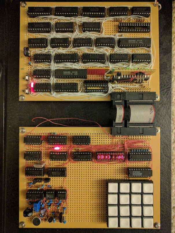
The program counter is composed of parallel-loadable counter ICs (74HC161). Actually the schematics contain only 2 of them, but I extended the real implementation to use 4 of them, so the program memory space is eventually 64k. In order to load data into the higher 8 bits of the PC, an extra latch IC (74HC574) was added. This latch has to be loaded with the MSB prior to each JMP instruction, the content of it is loaded into the higher (MSB) counters at the same time when the lower 8 bits are loaded directly from the CPU internal data bus.
The PC is incremented automatically after each read from the program memory (fetch cycle, or reading literal data from program memory).
Instruction register
The instruction register is an edge triggered D latch (74HC574), this register is loaded with data during each 'fetch' cycle. The easiest way to imagine the fetch cycle is as a special hardwired MOVE instruction; the data source is always the program memory and the data destination is always the instruction register.
Instruction decoder
The instruction decoder is composed of two demultiplexer ICs (2 x 74HC138) and is driven by the instruction register. A CPU instruction word is 8 bits wide, 3 bits select the data source and 3 bits select the destination. Each demultiplexer ICs apply the control signals to the selected destination/source at the execute phase (3. phase).
The instruction decoders (2x74HC138) use up 6 bits of an instruction word, I used the remaining two bits for instruction modifications:
One bit indicates conditional (on zero) execution; when this bit is reset, the instruction is only being executed if the content of the accumulator is zero. I achieve this by simply inhibiting the data destination demux IC in case the aforementioned condition doesn't exist. When this bit is set, the data destination demux IC is always signaled, regardless of the content of the accumulator.
The other bit (missing from the schematic) is used to implement a tricky functionality; when set, the carry output of the adder is fed back to the carry input. Here's the use of it: the CPU doesn't have a bit shifter, the only ALU functionalities are addition and bitwise negation. If I wanted bit shifting to the left, I would need to add the content of the accumulator to itself. Where the carry feedback comes into picture is bit rotation; if I want to rotate bits, I simply add the contents of the accumulator itself and indicate carry feedback; the MSB will be fed back to the LSB and the result will be the same as bit rotation to the left. However I still cannot rotate bits to the right, so I have to write an algorithm for that; I rotate to the left seven times; and to be complete, I can do bit shifting to the right as well, by doing seven rotations and one shift to the left; and since I can compare two values (subtract and execute if the result is zero), I'm able to implement bitwise OR and bitwise AND algorithms too.
Not having native bit rotation, bitwise AND and OR support on any CPU is quite unheard of, but in reality these are the least utilized functionalities; from programming point of view, addition and subtraction are the most commonly used functions. I think it was a good choice to have native adder on the CPU and omitting basic logical functionalities, I haven't seen any homemade TTL PU on the internet yet that fits on a 4" x 4" board, and runs 64k C programs, and all this without microcode.
Opcode format:
    7        6        5        4        3        2        1        0
+--------+--------+--------+--------+--------+--------+--------+--------+
|Carry fb| On Zero|  Src_0 |  Src_1 |  Src_2 |  Dst_0 |  Dst_1 |  Dst_2 |
+--------+--------+--------+--------+--------+--------+--------+--------+
ALU and Accumulator data paths
All the ALU functionalities are implemented with two 4-bit full adders (74HC283) and an inverter (74HC540). Though the CPU only supports adding and bitwise negation, theoretically all the basic logic and arithmetic functions can be implemented by software, making this CPU fully Turing-complete.
The accumulator can be loaded with data via 3 different paths: 1) directly via the 74HC541 buffer, 2) via the 74HC540 inverter, 3) and via the adder. One of the operand of the adder is always the previous value of the accumulator; the other operand comes from the CPU data bus from any component (even from the accumulator, resulting in 'x2' or 'bitwise shift/rotate left' operations).
The zero detector is implemented by a 8-input diode-OR gate. Its output is evaluated when the conditional execution bit is set to zero in the opcode.
Other control circuits and peripherals
The CPU has a start-stop circuit (SR flip-flop made up of discrete gates) to inhibit the CPU clock and make the program memory available for programming. When stopped, the CPU phase circuit is kept in either phase 0. or phase 1. (MSB cpu phase latch is constantly kept in reset state). Since phase 1. is a fetch phase and PC is incremented at the end of each fetch phase, making a phase 1. -> 0. transition by toggling the PC_INC button is the simple way of incrementing the PC when entering the program. Program memory can be written only in phase 0. so PC_INC button has to be toggled twice after each write (it's not elegant but the implementation was very simple).
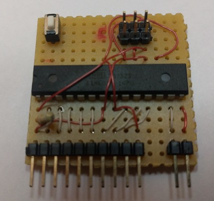
(UPDATE: I created a simple programmer hardware based on the ATmega8 MCU and eliminated all the programming buttons. This programmer plugs into a socket and transfers the bytecode into the CPU program memory on each startup. The programmer can be deattached after programming the CPU.)
There's no separate input port circuit/buffer on the CPU; a series of 100k resistors transfer the logical state of the input port to the internal data bus when the output of all of the other components are in Hi-Z state.
The clock source is a basic variable-frequency relaxation oscillator, constructed of a Schmitt-trigger (74HC14), a capacitor and a trimmer pot. One more Schmitt-trigger is used for consolidating the PC_INC toggle button waveform, the rest four (74HC14) implement the discrete inverters used elsewhere in the CPU.
In the final design, I included an SRAM data memory too. I also added an address latch (74HC574), which has to be loaded prior to reading or writing to the SRAM.
The ATMega8 based programmer:
Programming
The CPU can be programmed with a custom toolchain that I created. It consists of an assembler, a C-like compiler and some miscellaneous tools. The C-like complier implements a basic subset of the standard C language with many restrictions (e.g. no struct, not arrays, no callback functions, no "strings", etc.., see this example) and the assembler is also basic, it just provides enough functionality to make the C-like compiler work on this platform. Originally I started writing the C-like compiler for fun under linux for the x86 architecture but I quickly adopted it to the TTL CPU after having realized that it would work if I also implemented an emulated stack.
The CPU doesn't have a stack pointer, nor it has stack manipulating instructions (push, pop, call and ret), therefore I implemented the stack functionality with some basic assembly macros. (see mcc/arch/ttlcpu/header.asm in the toolchain). One of the upmost memory locations is appointed as stack pointer, the macros basically load the value of it into the accumulator (after having saved its content if necessary), increase/decrease it then store it back. An additional trick was needed for the 'call' instruction, where the return address has to be stored on the stack; I just use individual labels that point to the next instruction after the 'call' and store it on the stack.
Overall, each stack manipulating instruction is carried out by 12-14 CPU instructions, therefore using them is extremely memory consuming; normally these functionalities are in microcode, the programmer doesn't have to tell the CPU what to do exactly each time a functionality is called; however with 64k address space it's hard to deplete the program memory and the CPU remains simple and its architecture is fully defined by hardware.
The CPU also lacks the standard ALU but it has everything to calculate any basic arithmetic and logic functions. The bitwise AND functionality is implemented in a subroutine (that is, the compiler actually calls it with 'call' instruction) as it would be too large to put it inline into the program at each invocation as a macro (it's a 64 step algorithm, see mcc/arch/ttlcpu/header.asm for details)
Peripherals
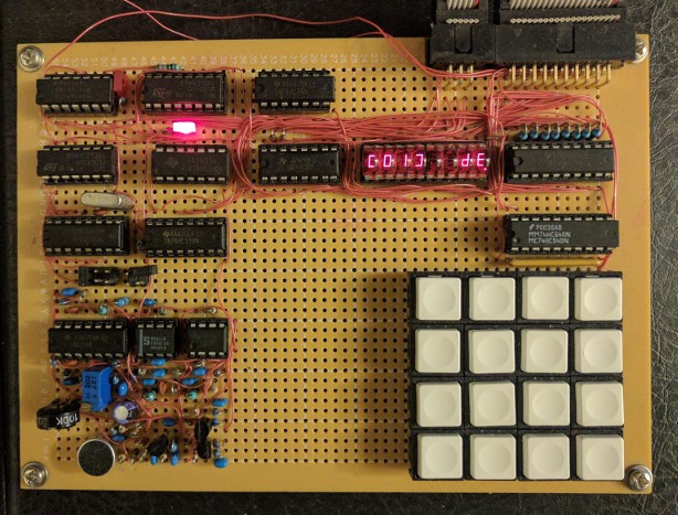
I created a simple 7-segment LED display interface and a keyboard interface on a separate board (you can see it on the video) and installed ribbon cable connectors on each board to interconnect them. The display and keyboard scanning routines can be found in 'mcc/arch/ttlcpu/header.asm'. The board also features a 8-bit serial receiver and a 300 baud FSK modem (with an electret microphone) that I plan to use as an input / program source for the CPU. The serial receiver can be configured for 300, 600 and 9600 baud.