 Ted Yapo
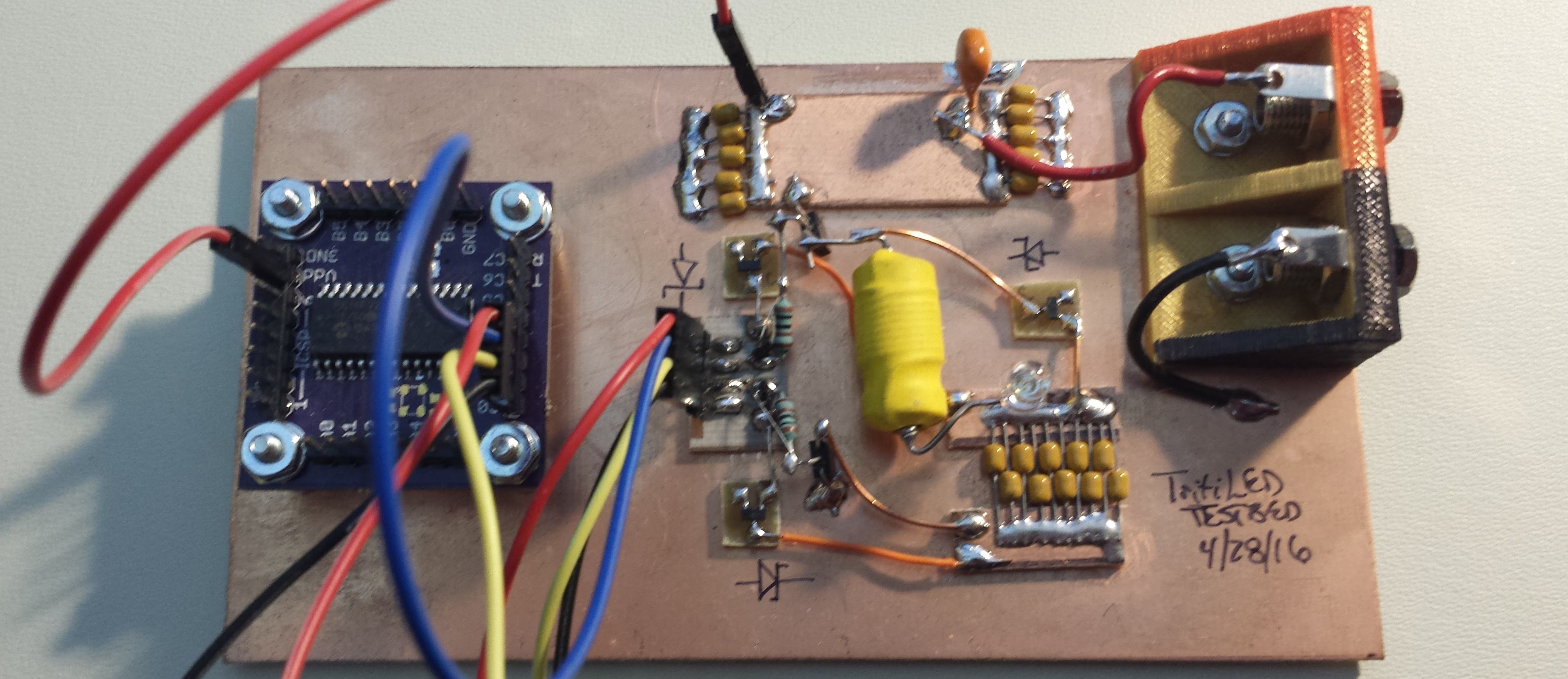
I actually prototyped a Version 2.0 back in April. I got distracted by some other things - like starting to use hackaday.io - so dropped it for a while. Here's the ugly board:
As I discussed last time, simply replacing the high and low-side drivers with more efficient MOSFETs is likely to cause more problems than it solves, because the LED current will become difficult to control. But what about replacing the drivers and adding an inductor to regulate the current pulse? Here's the idea (but not what I actually prototyped):
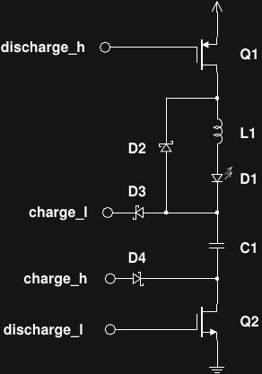
Q1 and Q2 are low-Rds MOSFETS. L1 and D2 have been added around the LED. While Q1 and Q2 are conducting, current builds through L1 and D1. Once Q1 and Q2 turn off, the inductor current continues to flow through D1 and D2 until the inductor is de-magnetized. The LED current pulse will then be triangular, with the maximum value (and total LED power) a function of the pulse width (assuming the inductor is large enough to stay out of saturation). The integrated LED power is now a function of the square of the pulse width, which might make a variable-output version a little more difficult, but maybe some software on the PIC can handle that.
The four inputs are driven from four PIC output pins. Here are the proposed waveforms:
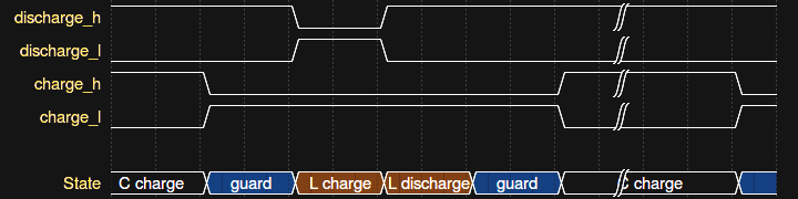
During the normal (non-pulse) state, C1 is charged through D3 and D4. Just before a pulse, the charge lines are switched to their respective "off" states to avoid any possibility of shoot-through (imagine what happens if charge_h and discharge_l are both high simultaneously). This "guard" time before the pulse need not be very long. After the guard time, the discharge lines are switched to their "on" states to start energizing L1. Current continues to build through L1 (and D1) until the discharge lines are switched "off" - this forms the first half of the current pulse. At that point, the second half of the pulse consists of the energy in L1 flowing through D1 and D2. A second guard time is shown in the diagram, but it's not strictly necessary, as there's no danger of shoot-through after the pulse.
I called energizing the inductor "charging" and de-energizing it "discharging". Are "magnetizing" and "demagnetizing" the proper words?
Back in April, when I built the prototype, I used ZTX618 and ZTX718 BJTs for the drivers, because I didn't have suitable MOSFETS. The problem with BJTs on both sides is that the base charge storage time stretches the pulse, making it difficult to control the pulse width. I ended up using some Schottky diodes across the base resistors to increase the turn-off speed, but stopped short of implementing full Baker clamps - at that point, it's time to use MOSFETs.
I ended up simulating the BJT circuit in LTspice. Here's how it looks there:

And the resulting simulated pulse:

The pulse width is somewhat arbitrarily set in this simulation run, but you can get the idea.
You can download the simulation file for LTSpice here.
I played enough with the prototype to see that it "worked," but not enough to get solid data. I figured that I'd switch to MOSFETs before really evaluating the idea. I have a test PCB with built-in instrumentation mostly designed, but I'm going to revisit it to use some more modern PICs in light of Jaromir's findings about the overall efficiency gain with newer devices. It's time to finish that PCB design and send it out.
Discussions
Become a Hackaday.io Member
Create an account to leave a comment. Already have an account? Log In.
Gate capacitance in the MOSFET can be a limiting factor on the riser/fall time for narrow pulse without a proper driver. You have to be using MOSFET with small gate capacitance that can be driven directly quickly with only tens of mA of gate current, but low enough RDS.
May be paralleling 74LVC bus transceiver gates as drivers for LED?
Are you sure? yes | no
Yeah, that would be a classic mistake on my part - and the second time I've fallen into that trap :-)
Over on #The Diode Clock, I needed to switch MOSFETs very rapidly - how quickly one forgets the pain! I ended up switching STP27N3LH5's (27A power devices) with a rise time of less than 10ns (the datasheet shows 22ns typ.). They only had 4.6 nC total gate charge and 475pF input capacitance, but it still wasn't easy, and took some hefty BJTs to pump out enough current. But, I can't use such a brute-force approach here.
I ordered some smaller MOSFETs for testing on this project, but they're all still around 3 nC total gate charge and 250 pF input capacitance, so it will be a little easier, but not much. Optimistically, there's a factor of two improvement in the raw devices. If(!) I can accept switching speeds of 1us, I can cut the current drive by a factor of 100. It's all right on the edge, but it might work.
I thought about using hefty gates as drivers - I'm fond of 74AC devices at higher supplies and when power isn't that much of a concern. A quick look at an NXP 74LVC245A datasheet shows 0.1 uA typical supply current - (good), and 10uA max (not so good). It also has a typical off-state output current of +/-0.1uA (+/-5 max), which could also be a factor. On the other hand, it has 8 gates each of which can drive +/- 24mA - not bad, although I need to check the Vol and Voh figures at those currents. This, too, seems like it might work, except at extreme temperatures, anyway. It's a good idea - thanks for suggesting it! I added a few of them to my current shopping cart; next time I order parts, I'll get some to try.
I do have some 74AUP inverters, spec'd at 0.5uA max quiescent (I think it's the lowest you can find) that I was going to try in a different experiment, but they're only 4mA drivers.
EDIT: I could also switch the power to the 74LVC driver itself with a stout high-side MOSFET - who cares how long it takes to switch power to the 74LVC part. Once it's powered up, it can generate the pulse quickly, then the power can be shut down again.
Are you sure? yes | no
I used Dual PMOS: DMG1023UV for power management on my hearing impaired project. Bad news: SOT563 - I had to alter the footprint for my Chinese PCB CM.
RDS: 1ohm
Input Capacitance Ciss: 59.76pF
Total Gate Charge Qg: 622.4pC
There is a complementary Dual NMOS with slightly better spec: DMG1024UV
I also used a NLAS4157 (On semi) SPDT Mux as power switch for pager motors. Around 1.4 ohms at 2.7V and 100mA (goes down to 0.3R at 4.5V). There is an enable and a tristate pin.
I picked them for price and performance and unfortunately not so much for easy to prototype.
Are you sure? yes | no
Thanks for this! A quick look at the datasheets, and they look like they could certainly work in this application. A handful of them found also their way into my shopping cart.
I have a bunch of #Ugly SMD Adapters coming in the mail today (supposed to be here yesterday). No SOT563 ones, but I could design one, send it off to OSH Park, and let the PCBs and MOSFETs race to my house...then prototyping isn't that hard.
Are you sure? yes | no