 Will Long
I have created a proof of concept FPGA in Verilog. The architecture overview is the image with the squares. Design choices were made at this stage based on ease of implementation. I started this out of curiosity but then it seemed to work. I'll explain my choices as I go.
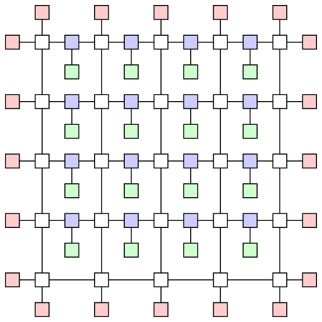
The channels in the routing fabric are three wires wide. Each wire is bidirectional; the direction is selected by configuring the switches in the routing and switch blocks. Originally I used monodirectional wires, but I switched to bidirectional wires after realizing how much monodirectional wires complicate the switch/routing blocks.
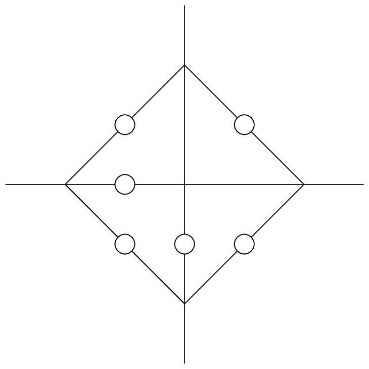
All switches in the design are currently based on tristate buffers. Two tristate buffers are wires in anti-parallel, and turning one on and the other off allows the signal to propagate in a particular direction. This is the best I think I can do in vanilla Verilog. Eventually I can use something more area efficient. Generally six of these bidirectional switches are arranged around four wires, to allow them to connect in various ways/directions. Below is a diagram showing the location of the switches.
I chose to use disjoint routing blocks (white squares). They don't allow all possible connections to be made between the ports, but they only need three switches. They were definitely the simplest to implement. Below is a diagram showing the location of the switches within the block, and a diagram showing the possible connections in a disjoint routing block.


The switch blocks (blue squares) are a three by three matrix of switches. These connect the logic cells to the routing fabric. There are no connections at the top, only the bottom (logic cell) and sides (fabric). Below is the diagram of the switch block.

The logic cells (green squares) are very simple right now. They have a four-entry look-up table, a switchable D-flipflop, two inputs, and one output. Each cell can only emulate a two input function (basically a single logic gate). Adding functionality to the cells is not too hard. The only complexity is adding more wires to the fabric when the number of inputs and outputs increases.
The components were connected in rows, then row by row from the bottom up. The IO blocks were wired last.
I tested all of the components in isolation except for the switch block. I also tested the entire FPGA, routing a signal from the bottom to the top. More comprehensive testing is needed. The logic blocks and their integration with the fabric hasn't been tested yet (although they work on their own).
I used Icarus Verilog to compile and test this project. I would like to move to SystemVerilog (for correctness) and/or Verilog A/MS (for features vanilla Verilog can't handle). I am also interested in implementing some kind of heterogenous architecture. Some logic cells can be replaced by DSP or other circuits. As I am a biomedical engineer, I would like to use this project as the basis for medical instrumentation.
There is no code uploaded because I'm still figuring out licensing. I'm not sure what the best license would be.
Thanks for taking a look!
Best,
Will
Discussions
Become a Hackaday.io Member
Create an account to leave a comment. Already have an account? Log In.