Now that we have a transducer (subject to change of course), we have to use that transducer to convert light into a number displayed on a computer screen.
There are two parts of that solution: the analog part and the digital part. In this entry I will just focus on the analog part because that is the more tricky part.
The big issue with this sort of power sensor is the dynamic range of the signal.
We need to measure signals from say 10 nA to 10 mA. That is 6 orders of magnitude. There is more than one way to attempt to solve this problem. Like most engineering problems there are advantages and disadvantages to each solution.
Whenever I see the phrase "orders of magnitude" I immediately think: log. After all if I need to plot a signal that ranges over orders of magnitude I will probably use a log scale.
As mentioned in previous in these logs the photodiode is essentially going to be a current source. If we could create a circuit that created a voltage that was proportional to log(I) then we could "compress" the dynamic range of this measurement.
Logarithmic amplifiers do exist. One log-amp I have used in the past is LOG101. It is a cool circuit.
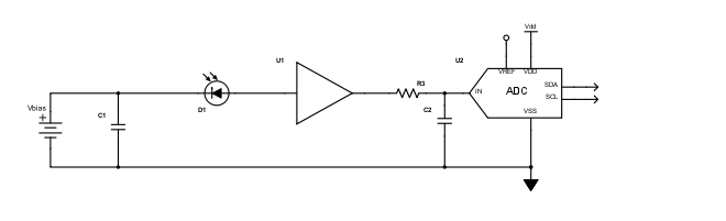
If we wanted to use LOG101 to solve our problem the circuit topology is pretty simple. We reverse-bias the photodiode and feed the current into the log-amp, which converts the current into a voltage which is then sampled by an ADC and sent to the digital part of the circuit using I2C in this case.
At first glance it seems a great solution. The tripping points to implementing this idea largely are in making a precision reference current for the log-amp. If you take a look at the LOG101 datasheet you will see the output is actually the log of the ratio of two currents, one of which is the reference.
The other downside to using LOG101 is that it is a dual supply circuit. If this device is to be powered over USB then only +5V is available. DC-DC conversion can be used to create a -5V supply (probably using a charge pump) but it certainly would complicate the system, cost more and potentially be noisy (it can be a task unto itself to get switch mode power cleaned up nicely for such a sensitive measurement).
Let's return to the original problem, we need measure a signal that ranges over 6 orders of magnitude. One way to look at this problem is how many bits is that? This is log2(1e6) which is about 20-bits.
Log-amplifiers are nice but modern analog to digital converters (ADCs) have huge dynamic ranges. They are available in 24-bit flavors. In principle this means just a resistor and an ADC could solve the problem. In practice the input to an ADC should at least be buffered.
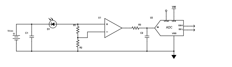
Taking this view it is possible to come up with this circuit. The amplifier (U1) is an instrumentation amplifier. Resistors R1 and R2 take the current from the photodiode and turn it into a voltage. If the value of R1 is well known then the current is known and from the sensitivity function then the power incident is known. The value of R2 may be 0 or it may be some fraction of the total resistance R (R = R1 + R2). If we place the negative terminal of U1 at the rail (0 V) then my suspicion is that performance will not be as good as if it is lifted off the rail slightly. This is the point of R2. Amplifiers can be rail-to-rail, but near the rails performance will never be as good. R1 sets the V/A gain, it is limited by the maximum current we expect to have output from the photodiode. This is of order 100 mA, given our rail (without DC to DC conversion) is at most 5V this implies 50 ohm is the nominal maximum for R.
If the instrumentation amplifier had a fixed gain this would also mean that it must be set low enough that the output voltage is acceptable to the ADC (which will have an input voltage range). Because 5V is the absolute maximum voltage in the system this implies a gain of 1. Thus we would have to rely solely on the ADC for the needed dynamic range (20-bits).
This is possible but a better way would be to pick an instrumentation amplifier that has configurable gain. This would ease the burden on the ADC by log2 of the voltage gain.
LTC6915 has this ability. The other items to consider are the noise and offset of the chosen amplifier.
There are 3 kinds of noise: thermal, shot and 1/f. Shot noise occurs a very low currents due to the quantized nature of electricity. Thermal noise is power is proportional to the resistance of the circuit. Finally 1/f noise is noise that grows a low frequencies like 1/f, it has a variety of origins. In general CMOS input amplifiers will have the worst 1/f noise because of charge traps in the SiO2/Si interface. Shot noise can be a problem as the current from the photodiode drops to very small values. Thermal noise can be important if resistors in the circuit become large.
Amplifiers have all 3 types of noise. Amplifier circuits that provide for feedback (e.g. opamps) typically will parameterize their noise as an input referred voltage noise density and an input referred current noise. Typically FET (JFET and MOSFET) input amplifiers will have low current noise and higher voltage noise. BJT input amplifiers normally will have low voltage noise and high current noise.
If you wish to minimize the noise of the system then this matters when selecting the gain.
In the example topology above the V/A gain is provided for by R which is rather small at 50 ohms and thus thermal noise is not a major issue. The LTC6915 uses switched capacitor techniques to avoid 1/f noise and minimize its offset.
This brings us to the other item which is the voltage offset. In an ideal version of this circuit the "read" difference would be exactly the difference between the negative and positive terminals of the amplifier. In practice this is not possible and there is an offset in this differential voltage. As long as the offset is stable it can be trimmed or calibrated out. Instrumentation amplifiers generally will have very low offset voltages as their primary application is measuring small voltage differences at low frequencies. The LTC6915 has a maximum offset of 10 uV. In current space with a 50 ohm load that is 200 nA. This is an order of magnitude greater than ideal but the part does have very low drift of only 50 nV/C in offset, so it should calibrate out of the system.
The circuit we have been considering is very simple. Simple in low noise analog systems is normally a virtue. Ever component you add will increase the noise of the system. A downside to proposed topology is that the reverse bias in the photodiode changes as a function of the intensity of the light input. The reverse bias creates an electric field in the depletion region of the diode which helps get current out of the device more efficiently. As the reverse bias falls the sensitivity will change. How much is not possible to know without more details like the carrier lifetime, geometry and doping profiles of the diode, or if none of those are possible an empirical measurement of the device.
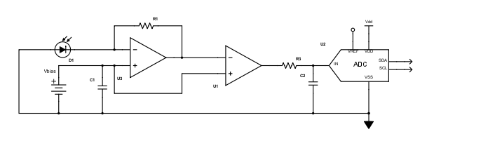 One way around this is to use the above topology. Here the first amplifier (U3) is configured as a transimpedance amplifier. R1 is now the nominally 50 ohm value. Independent of current the feedback in the circuit will keep the voltage across the diode at Vbias. The voltage at the output of U3 is now backwards with 0V being the maximum intensity and Vbias being the lowest intensity.
We still want the configurable voltage gain of the instrumentation amplifier (U1). We also want to flip the sign of the V/A gain and remove the offset voltage. This circuit does all these things.
To correctly infer the current from the photodiode it requires that the offset voltage of first amplifier (U3) be very low. This suggests that U3 should be a chopper amplifier. This is another type of amplifier that uses AC techniques and is good for low frequency and DC measurements.
Many amplifiers of this type exist but reasonable choices include: LTC2054 and OPA378. These both have desirable low-drift and offset properties. They also share a pinout for the SOT23-5 package. The typical offset voltage for the LTC2054 is 0.5 uV, the OPA378 is much worse at 50 uV. The noise of the OPA378 in a 0.1-10 Hz bandwidth (i.e. near DC) is 0.4 uVpp while it is 1.6 uVpp by the same figure of merit for the LTC2054. So while the LTC2054 is better at offset the OPA378 has better noise properties. Both of these amplifiers are relatively inexpensive, and single supply which makes them good for this application. Other choices no doubt exist with the sample pinout as well and could be swapped in later.
We just saw that a tradeoff could be made between noise and offset voltage with the circuit above. The offset voltage mattered because we had to assume that the voltage at the negative terminal of the first amplifier was the same as the positive terminal.
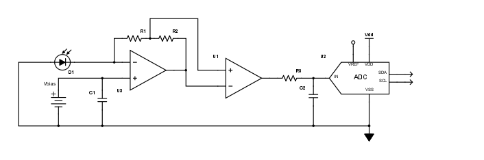
We could get around the assumption by doing something like the circuit above. Here the offset voltage of the first amplifier no longer matters. It retains the ability to keep the photodiode reverse biased at a constant voltage. Similar to the second topology discussed R1 + R2 set the overall V/A gain. R1 could be set to 0, however that places the input of U1 in a very sensitive part of the circuit. R1 provides some isolation from that point as needed.
If the instrumentation amplifier were ideal in terms of its input impedance (infinite) then this would be a good solution to decoupling the noise properties of the first stage from the offset voltage issue. However the instrumentation amplifier is not perfect. It will take some current out of the feedback path. Because the total R will be of order 50 ohms, it is quite likely this topology could work well because the effective input impedance of the instrumentation amplifier is much greater than this. Putting active components into the feedback path could be dangerous the the stability of the system.
Also any loading of the feedback network makes the current measurement we care about inaccurate by the current loss. This could for the smallest current levels.
If this topology were to be used a BJT based OPAMP with low current noise would be the best choice for the first stage (U3) due to the transimpedance gain required. An example of such an amplifier would be LT6230.
Comparing the last two topologies the second to last is nice because it is straight forward and predictable from the datasheets of the parts. Both amplifiers are designed with DC applications.
Considering LTC2054. With the mentioned parts the offset typically is 0.5 uV. This systematic error is of order 10 nA when used with 50 ohms. The dark current of the photodiode is several 3 nA typical and 7 nA maximum. So uncorrected this systematic error is larger. The noise power in 10 Hz is on order of 1.6 uV, this is more like 30 nA. Given the sensitivity function this places a floor to the measurement of around 300 nW for the worst case (0.1 A/W @ around 400 nm).
We also must consider that we have an offset error in the second stage with the instrumentation amplifier. The maximum value for LTC6915 is 10 uV but the typical value is -3 uV. Because we are trying to infer the current across the feedback resistor an error on the output node is equal to the error on the negative input and so this appears to be the dominant error if uncorrected.
If we do correct for the offset errors then we could use OPA378. In this case we would have noise equal to about 8 nA.
Using the last topology would reduce the noise further. For LT6230 a quick estimate for the Vpp in 0.1-10 Hz figure of merit used by the other two would about a factor of 3 lower than for OPA378, and thus well under the dark current.
So in summary, if the system can be fully calibrated for offset and the feedback is not significant disturbed by the sampling in the path, then the last topology is likely best. However the second to last is more certain to work and just as good if the extensive calibration for offsets is not done. As a result I will first pursue building the second to last topology, then if time allows I will work on the last version and see if it is indeed better.
Discussions
Become a Hackaday.io Member
Create an account to leave a comment. Already have an account? Log In.