 Arthur Admiraal
foIn this log, let's examine the electronics of the Rapid Impedance Spectroscopy Array, RISA.
Construction
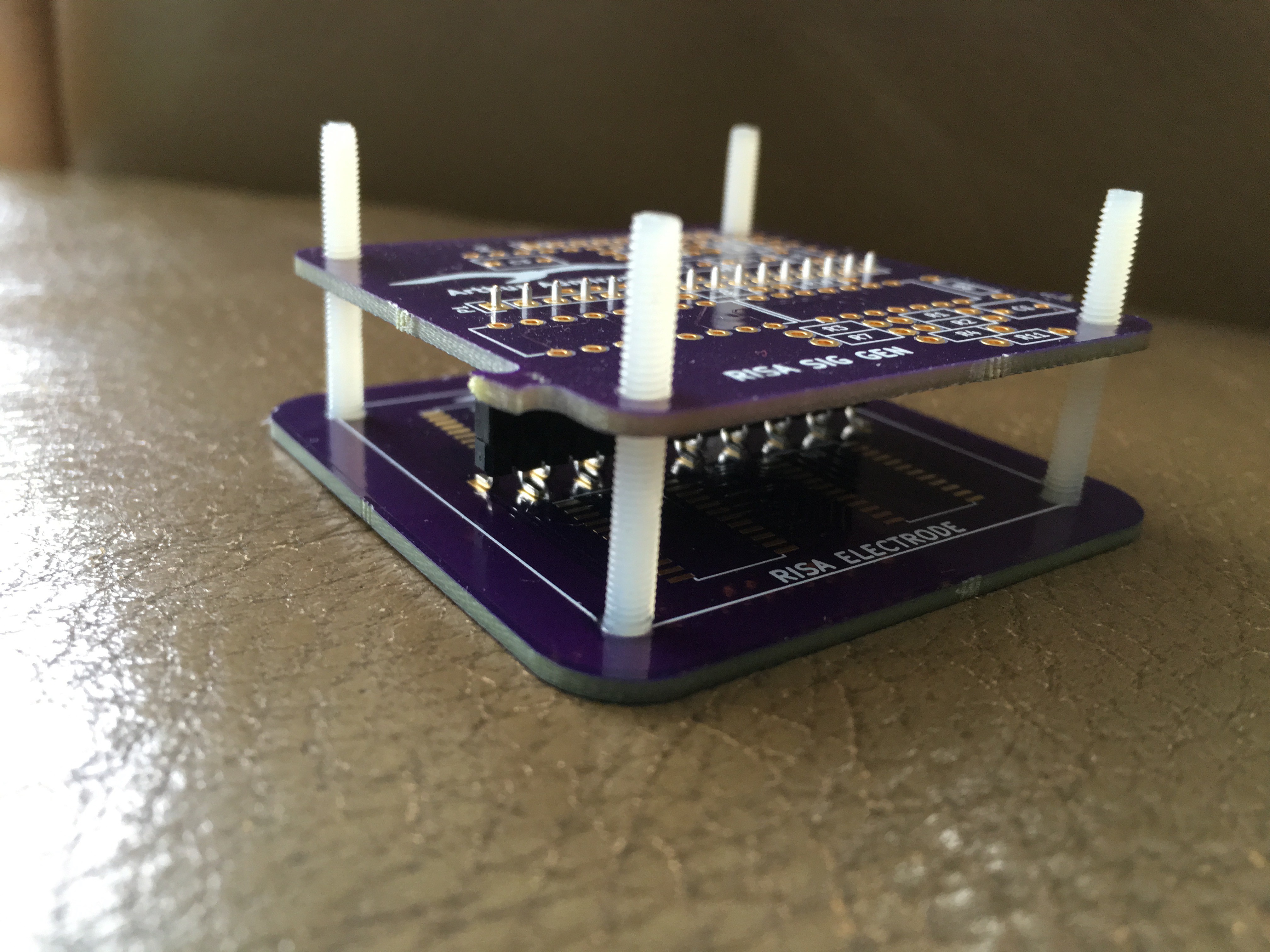
RISA consists of 2 two-layer boards, which are connected by .1" headers. The reason for having two boards is that the electrode board couldn't have any solder joints on the bottom, because those could influence the flow and provide a path for current to flow to other than the electrode pads. Since I wanted all signal generation hardware to be through-hole for easy experimentation, I needed a separate PCB for that.
The electrode PCB (the bottom PCB in figure 1) contains 64 electrode pads at the backside, arranged in an 8 by 8 grid. On the topside, there are 4 4067 multiplexer IC's. These had to be surface mount to fit them on, and to not violate the no solder joint on bottom rule.
The signal generator PCB (the top PCB in figure 1) contains some analog electronics and some headers, in which a Teensy 3.2 is mounted, which does all the signal generation, measurement and contains the smarts of this project.
I will go into more detail about how this is mounted in the log about the mechanical side of the project, and the construction process can be found in the build instructions section in due time.
What it does
I have been mentioning Electrochemical Impedance Spectroscopy a lot, but what is it exactly?
Simply put, EIS is a technique where you measure the impedance of a sample over a certain frequency range. This data, called an impedance spectrum, can then be used in a number of ways. It can either be used to characterise electrical systems, such as filters, but it also has applications to find the chemical composition of a sample. EIS is used as a non-intrusive way to measure fat content in people's legs for example.
But what is impedance? For this project you only need to know a few things about it:
- Impedance is basically resistance that changes with frequency.
- Impedance has 2 parts to it:
- An imaginary part
- A real part
This is a gross simplification. I recommend watching this video for getting a more thorough understanding of the concept.
At its core, RISA switches two electrodes in its array to an AC signal output and ground, and measures the resulting current. It then repeats this process for various frequencies to obtain an impedance spectrum. It also has control over the stepper motor driving the linear slider on which it is mounted, so that it can influence the flow speed and gather impedance spectra for various amounts of flow.
How it does it
The array
RISA will only ever need to collect impedance spectra between adjacent electrodes, and only horizontally or vertically. So when electrode that I've highlighted green in figure 2 is in use, the only other electrodes that can be used are the ones that I've highlighted red.
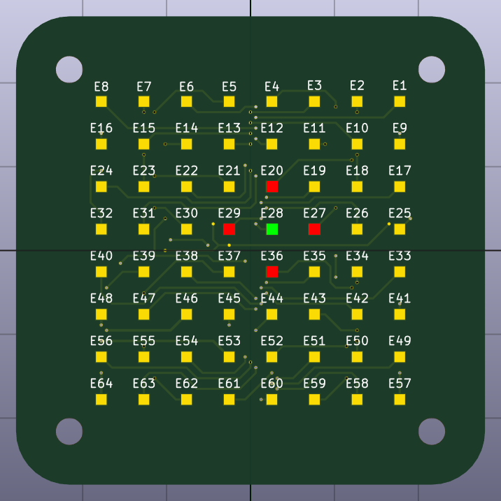
Figure 2: The adjacent electrodes.
So we don't need two grids covering all electrodes, we just need a chess-board pattern:
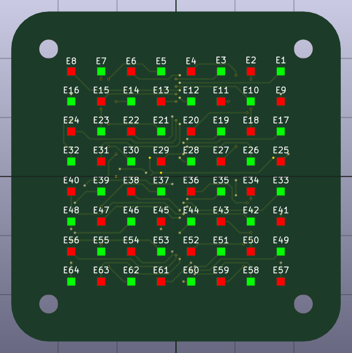
Figure 3: The two electrode selection grids.
We then need electronics to select any electrode on both of those grids:
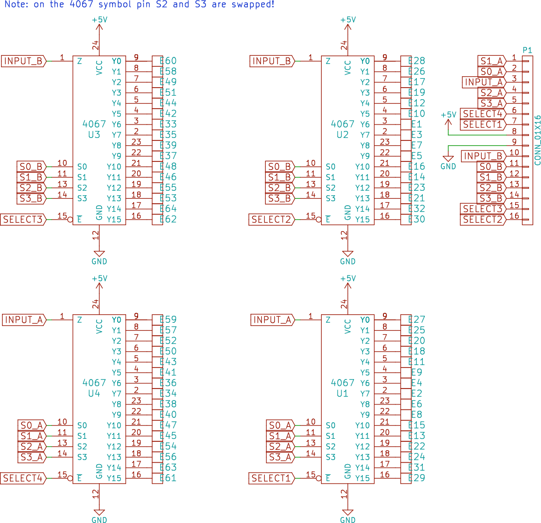
Figure 4: Electrode schematic.
For this, we use multiplexer ICs. If you're not familiar with those, they basically allow you to bidirectionally connect one or more inputs to one or more outputs. These IC's, the 4067, let you connect one input to 16 outputs. The S0 through S3 pins allow us to select which one, using a binary scheme. Using 2 of these, we can hook up every electrode in one of the grids to an input. But we still need to switch one of the 4067s off so that the input isn't connected to two electrodes. That is what the SELECT lines are for. Add another two, and we can connect every electrode in both grids to two inputs. These go off to the signal generator board, along with the digital lines used for selecting the right electrodes, via connector P1.
The signal generation
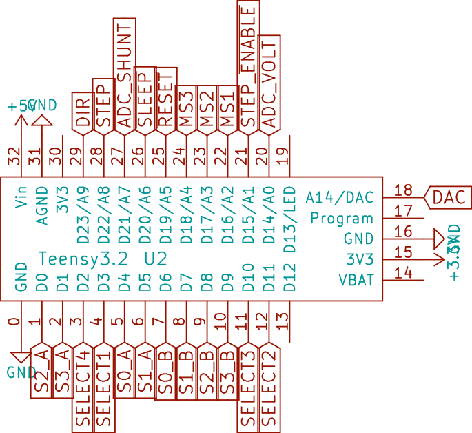
Figure 5: The Teensy 3.2 on the signal generator board schematic.
The signal generator board houses a Teensy 3.2. Almost all I/O of the Teensy are used. Some are used to switch to the right electrode, others to drive the stepper motor and others yet again for the analog signal generation and measurement.
The Teensy 3.2 has a 12-bit DAC capable of generating all sorts of waveforms. There is one problem however: it generates signals from rail-to-rail, or from 0V to 3.3V. This is an issue because we need an alternating voltage that goes both above and below ground. Furthermore, we don't want it to be this high, to prevent electrolysis in the electrolytic solution.
We can fix this problem by using some basic op-amp circuits. Instead of using the ground of our teensy as the ground reference for measurements, we can create what is called a virtual ground.
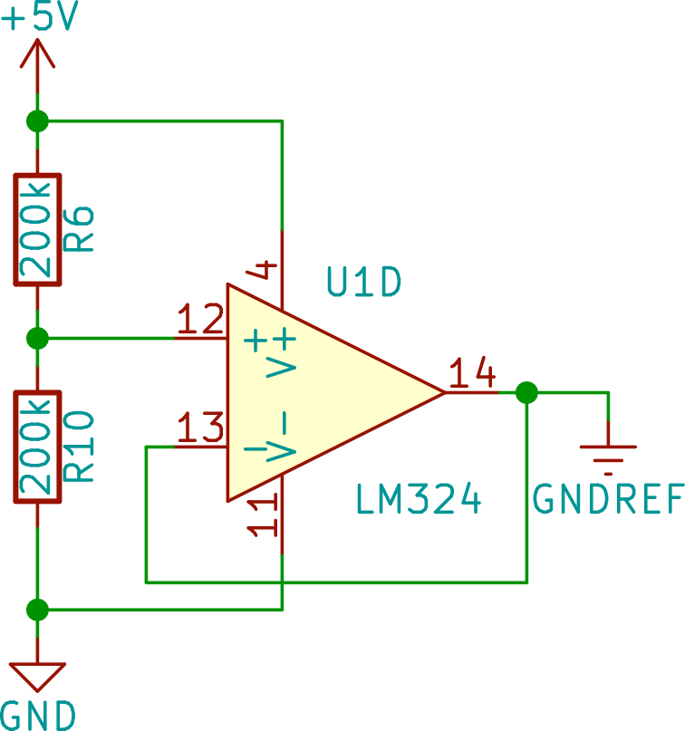
Figure 6: The operational amplifier circuit for creating a virtual ground.
This is done by simply dividing our supply voltage in half using a voltage divider, and buffering it with an opamp voltage follower circuit, so that the virtual ground is referenced by the current drawn from it. If we use this virtual ground, denoted by GNDREF in the schematic, we can obtain negative voltages relative to it, by just dipping below 2.5V, half the supply voltage. Our signal is yet centred nicely around this virtual ground however, and is still a bit to high.
We can fix this by adding a high pass filter and voltage divider:
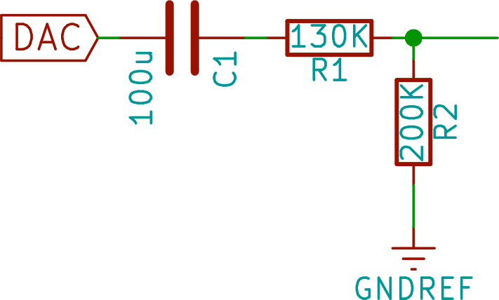
Figure 7: DAC Biasing and voltage scaling.
This works because the capacitor slowly charges up through the resistors to GNDREF, but allows our fast-changing measurement signal to pass through mostly unscathed. The signal is then divided down by R1 and R2 to 2V pk-pk.
However, if I were to even draw I tiny current from here, the voltage would drop dramatically, due to the high resistance. Also, how do we go about measuring the current? We can use another op-amp circuit to accomplish these goals:
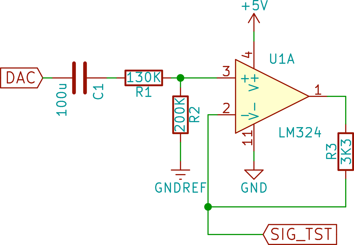
Figure 8: Signal buffering.
U1A Buffers the signal, like we did for the virtual ground. However, you may have noticed R3 in the feedback path. The larger the current being drawn by the solution, out of SIG_TST, the higher the voltage drop over R3 will be. Thus, we can use this drop to determine the current. The test signal doesn't drop because of this, since the op-amp will compensate for the drop since its negative input is connected after R3.
So that is our signal generation complete, but how do we go about measuring the current?
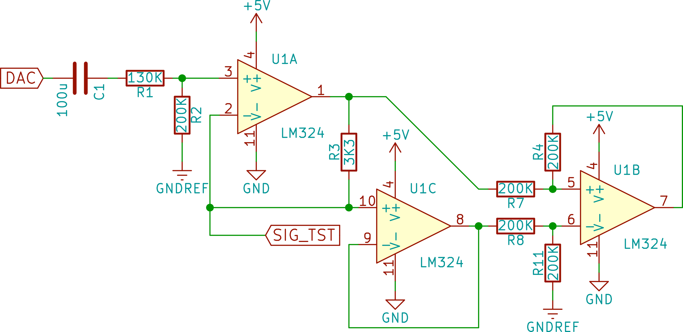
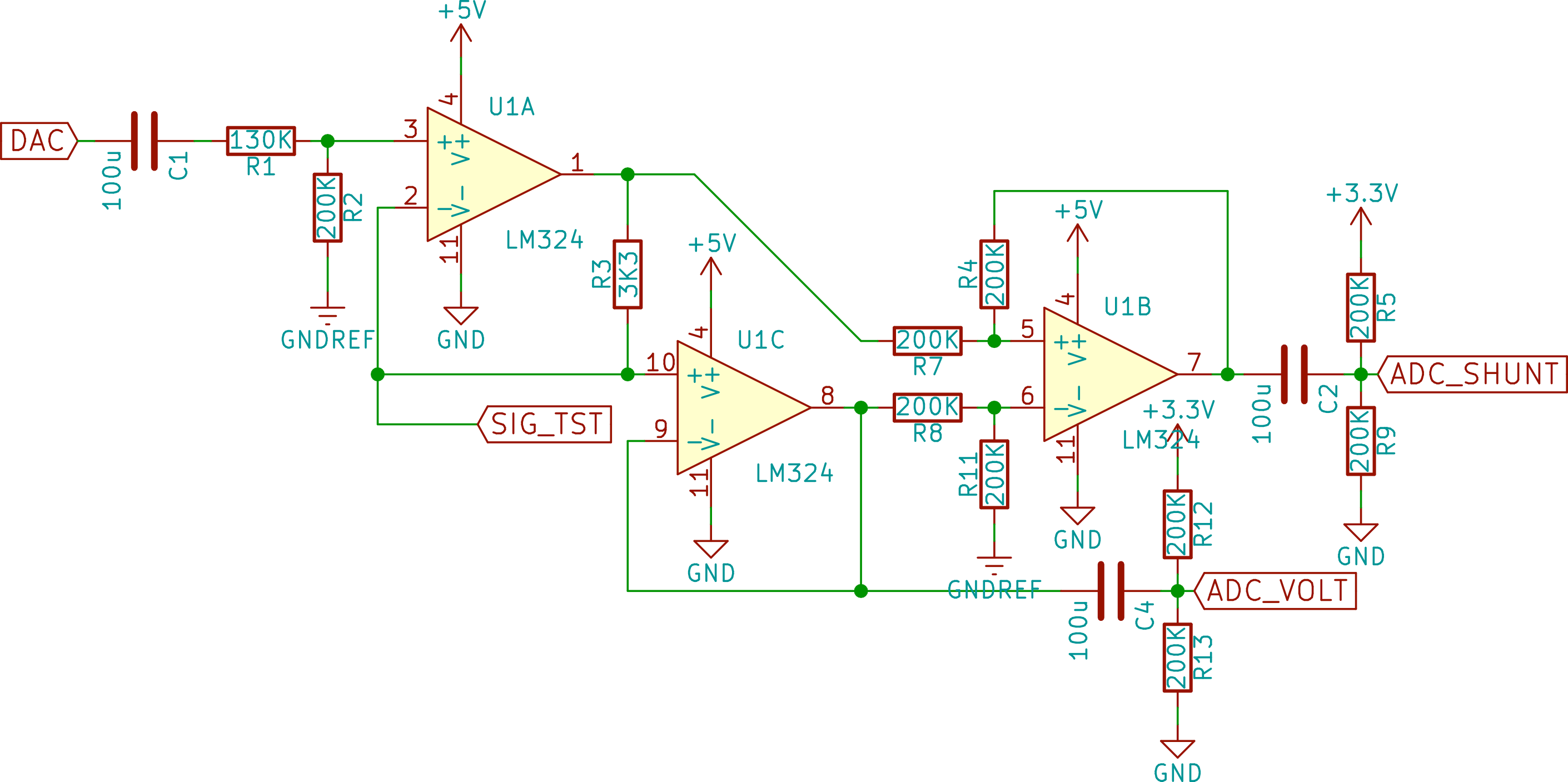
Figure 9: Buffered differential amplifier for current measurement.
That's right: more opamps. We can use a differential amplifier circuit (opamp U1B) to find the voltage over the resistor. We use GNDREF instead of the normal GND for the negative input to make sure negative currents can also be output. We buffer the test signal with U1C, since even the tiny amount of current that is drawn by the resistors connected to the negative input of U1B of about 5 uA is a significant impact on our measurement. Also, since opamp tend to come in either single, dual or quadruple packages, we would have had this opamp leftover anyway, so this is a good place to put it to use. The signal going to the positive input of the differential amplifier doesn't need any buffering, since it comes straight out of U1A, which has a low source resistance.
There is still one problem left: the signal put out by U1B is centred around GNDREF, 2.5V, while our ADC measures until 3.3V. To utilise the maximum dynamic range of the ADC, we need to bias the signal again. Also, since the Teensy 3.2 has two ADCs, why not use the second one to check on our test signal by tapping off the output of U1C. The completed circuit then looks like:
However, there is still more to talk about. I want to be able to obtain an impedance spectrum in both directions. To do this, you just need to add another switcher to the circuit:
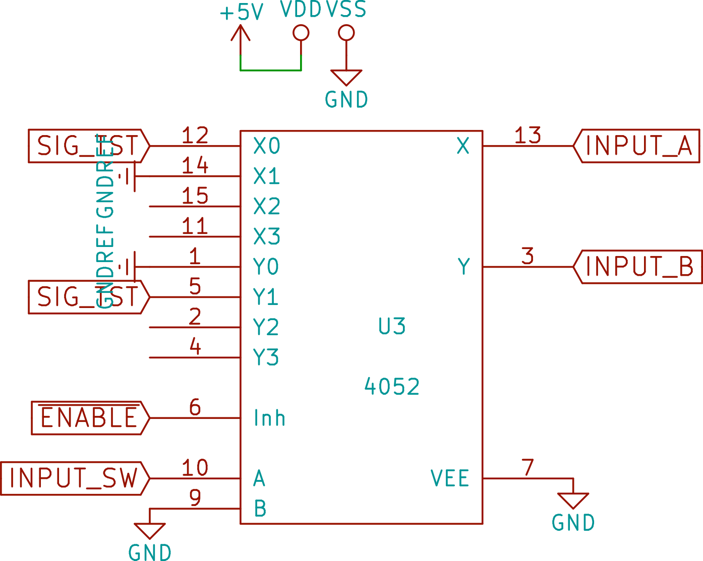
This chip has way more inputs than needed, but by connecting switch input B to ground, we only select between X0 & Y0 and X1 & Y1. By connecting the opposite signal to Y0 as X0 and Y1 and X1 we can switch the inputs of the electrode array grids to the desired signals.
Well, the rest of the signal generator board is just some connectors and decoupling capacitors, so that the whole schematic of the signal board becomes:
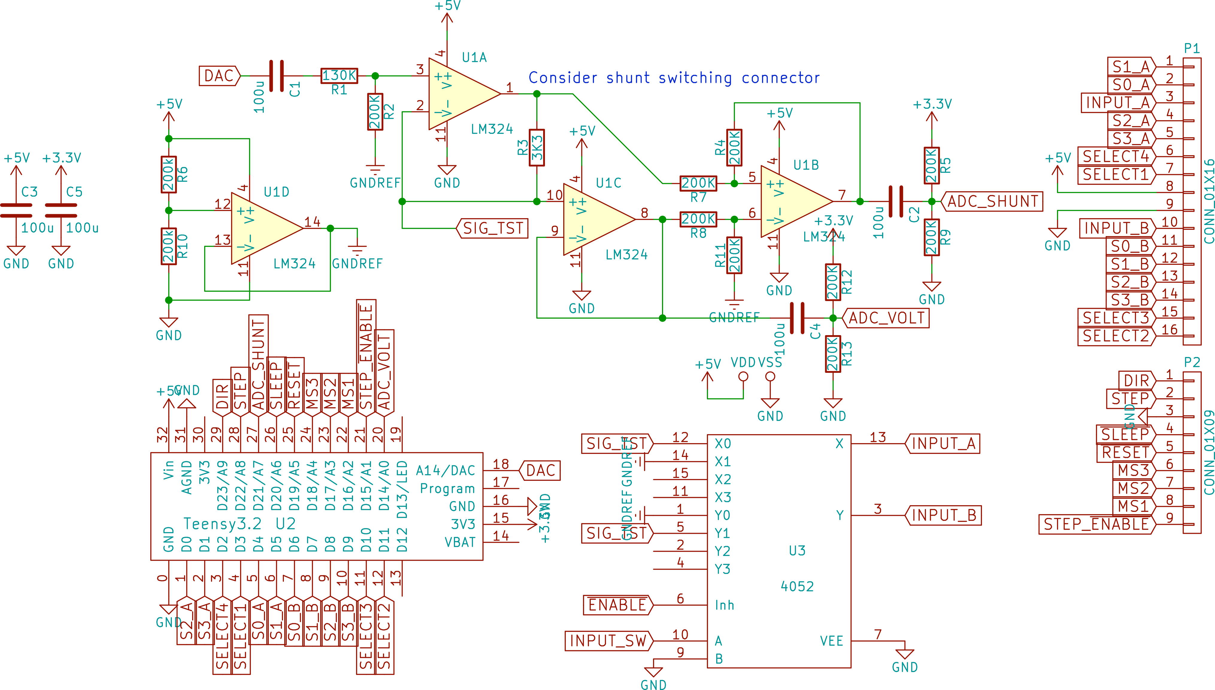
Figure 12: complete schematic of signal generator board.
Well, that's it for the electronics. Hopefully, you learnt something new, and if not, at least you know what makes this design tick.
Discussions
Become a Hackaday.io Member
Create an account to leave a comment. Already have an account? Log In.