 Dan Kisling
Let's jump into the simplified system block diagram for our spectrum analyzer. What is posted below is actually our revised system block diagram. Our first diagram had a few components we decided to eliminate, and while it is good to learn from our mistakes, it is also good for to avoid writing a novel on how to build a spectrum analyzer.

To elaborate further on the picture, the differential signal comes in through probes to a digially controlled amplifier (so the user can increase the gain in order to see smaller signals on the device). From there it is passed through a digitally controlled oscillator. We used the LTC6903 as it was easy to use. Astute readers might point out that in the last log I said sinusoidal signals, and the LTC6903 produces square waves. They are correct, but a square wave is just a sine wave with extra harmonics. As long as the harmonics don't distort what you're doing (as they are eliminated by the bandpass filter) why not use square waves. We found that square wave oscillators were easier to control and cheaper to buy.
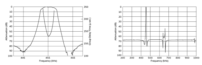
After the signal is multiplied by different frequencies it goes through a really sharp bandpass filter. This bandpass filter is awesome. We tried to design our own, but found it was really hard to not significantly distort the signal. Our adviser suggested we look to see if there was a cheap part built for AM radios that could work for us. And sure enough, for a couple bucks you can have a really impressive passive bandpass filter. I mean, check out the frequency response to this thing. It's about as close to a brick wall filter as I've ever seen.
 After the bandpass filter, the signal is sampled by the ADC. Everything from there is done in software. The raspberry pi takes the samples and performs a GPU accelerated FFT on them, splices the spectrums together, and displays them in the GUI to the user. The user can then use the GUI to change some settings in order to capture the signal he or she wants.
I'll elaborate more on this point when I discuss the hardware design, but we also broke out a second signal path in our PCB. By moving some jumpers, you can get the signal to come straight from the digitally controlled amplifier straight into the ADC. This allows someone to sample a signal in a straight forward manner, without all of the superheterodyning fanciness.
That's all for now. In the next log I'll talk a little bit on simulation of our technique to test its feasablility.
Discussions
Become a Hackaday.io Member
Create an account to leave a comment. Already have an account? Log In.