 Chuck Glasser
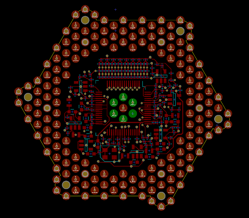
So here is what the final ADS1299 Layout looks like.
As a point of reference for scale, a poker chip just fits within the boundary of this pattern.
So something of an explanation. If the circuitry were missing and there was only the pattern of pads, each 2mm in diameter, then there are 241 pads per side. for a total 482 possible points of signal or power connection. That's a lot of pads!
The artwork looks like this.
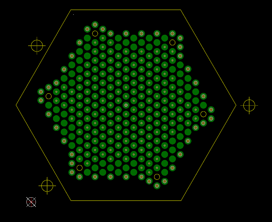
It looks like that on the other side. Take my word for it.
So the ADS1299 circuitry within a token is encapsulated top and bottom by two surfaces with this pattern.
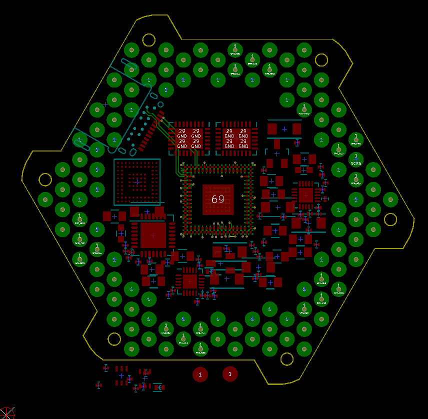
The data switch looks exactly, well almost exactly the same.
All the components in the system look the same. Just a bunch of tokens that are stacked on top of each order. With nothing to distinguish them from each other, other than a hidden code known only to wizards such as myself.
Each token, having it's own special function while also having the ability to communicate with other tokens anywhere within the system.
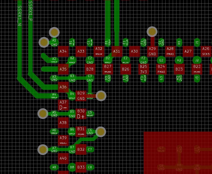
That's a USB3.1 C connector that offers 100 Watts of power and 40 Gb/s, the FPGA, a Xilinx XC7A35T in a CPG236 package. The layout follows 4mil design rules.
Here is the really great part. Check out how nicely the XC7A35T Artix FPGA matches up against what I think is an absolutely great embedded processor, the PIC32MZ.
The PCB capture is done using Kicad. Really, really like Kicad!! I've used many PCB tools in my career, Kicad is very nice. Takes practice like most things to be effective. After a time I've begun to understand it's quirks.
This graphic illustrates how nicely the FPGA in green marries up against the PIC32MZ in red using 4 mil design rules.
Each of the devices discussed so far is about the thickness of a poker chip, with similar weight. So, if you stack them in the correct order. That would be, electrode, electrode amplifier, and switch, then there is a complete signal processing chain going from a simple, multichannel precision, low level differential voltmeter, to an interface that in theory does 40 Gb/s. A system of instrumentation that is literally so fast that data from a whole array of sensors disappears into the data cloud within a single clock cycle of the original sensor data clock.
So, back to the electrodes. Now that I know what the pattern of contact for the electrodes are, as expressed in the ADS1299 circuitry, I can proceed on the layout of the LTCC artwork.
Discussions
Become a Hackaday.io Member
Create an account to leave a comment. Already have an account? Log In.