 Ted Yapo
I haven't been good about updating this project, but I've been using these adapters very successfully. Most recently, I've started adding castellated edges for soldering to the ground plane. Here's a look at some under the 10x inspection microscope:
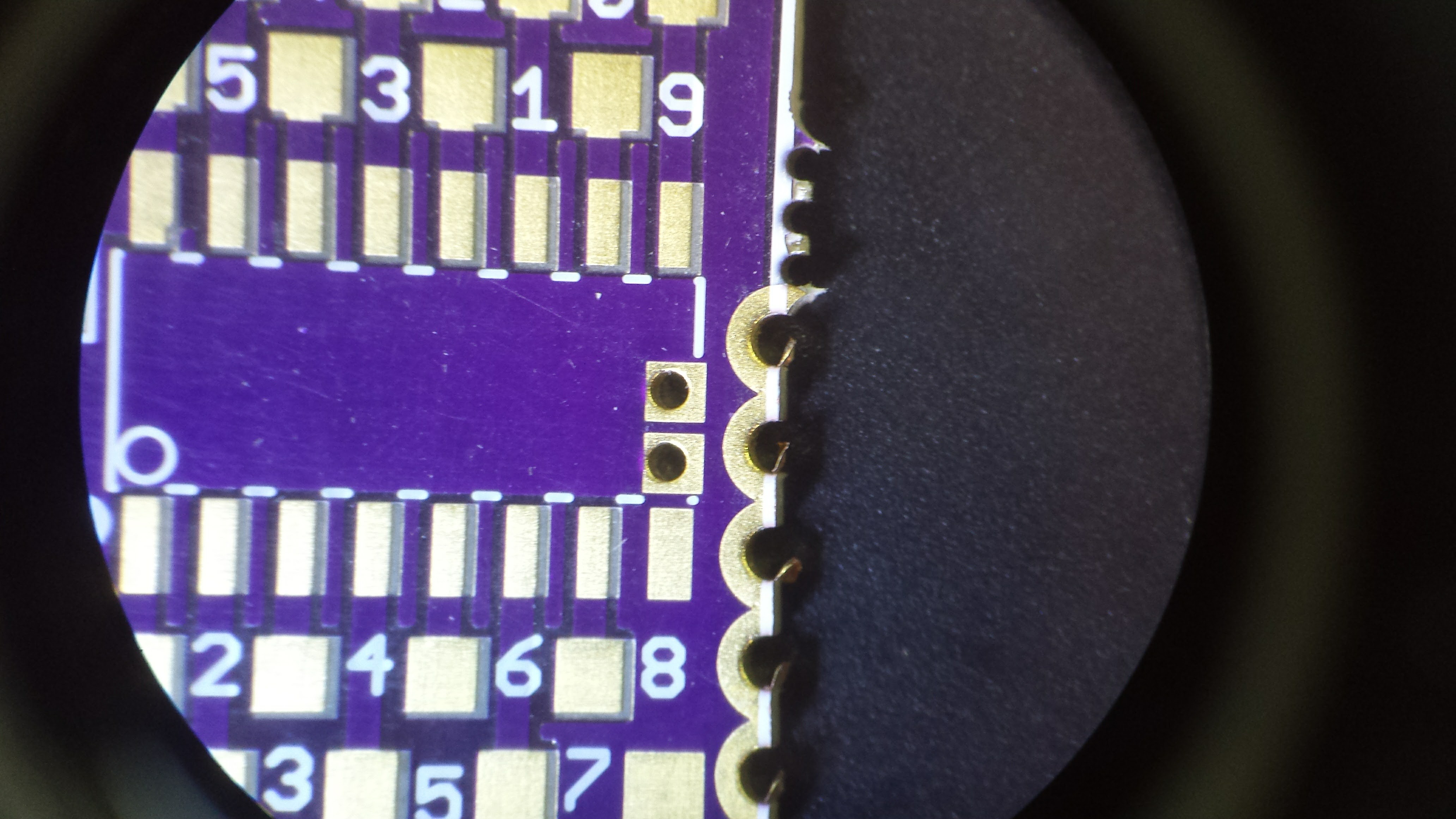
This board was (obviously) made at OSH Park, using their castellation guidelines. As you can see, the outer cut can leave a little bit of extra copper foil attached to the hole. This is easily removed with a knife, a file, or sandpaper. If you were using these for connecting individual signals to a base board, you would probably want to remove them before soldering to avoid possible bridges. Since I'm using them for ground connections, I didn't bother, and just soldered them to the ground plane as is. The result isn't particularly attractive, but it works:
These particular adapters were made for SOIC logic packages for the #PIC Graphics Demo. The project uses 74AC logic, which has a reputation for causing trouble with ground bounce and with signal reflections due to very fast edge rates. As a result, systems built with 74AC can be more sensitive to layout than other logic families. I wasn't sure how well the castellated ground connections would work, so I also removed the soldermask from the bottom ground plane on the adapters:
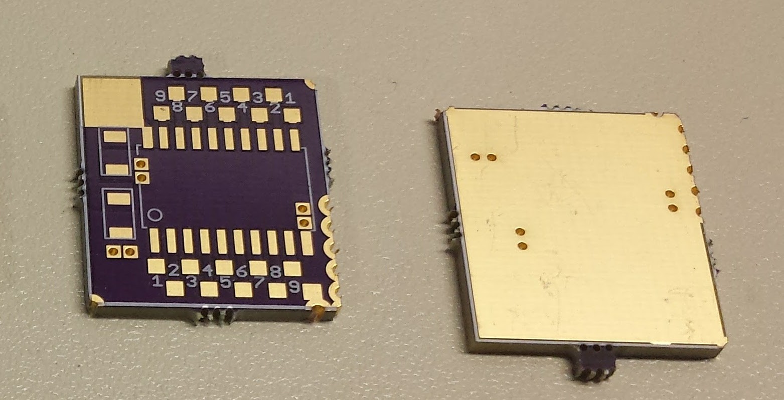
The idea is that you could reflow these adapters to the solid copper clad ground plane if you wanted. As it turned out, just connecting the grounds with the castellations worked for this particular project - although the bare gold is right next to the bare copper, closely coupled capacitively, if not conductively. I don't know if it would work for everything. For 74HC gates, there should be no issues just connecting the castellations.
As you can see in the image, there are sites for bypass capacitors on the boards; they assume the standard corner power-pin layout of logic ICs. In that sense, they're not totally general-purpose, but they could be used for any logic gates in standard packages.
The solder pads are 50 mils square, and spaced 100 mils apart. This is a comfortable pitch for me to hand-wire boards with wire-wrap wire - the 50 mil pitch of the SOIC parts is just a little too small.
One thing I want to try is making adapters for wire-wrapping SOIC gate packages. Some ICs are no longer available in DIP packages, and wire wrap sockets are very expensive. Adapters that mounted SOIC parts and 25-mil square gold header pins would solve both problems. Also, the low-profile of the SOIC parts would let you mount the pins on the top side of the board, with room to wire-wrap over the ICs - where did I see this around here? No more reversing the pin layout in your head!
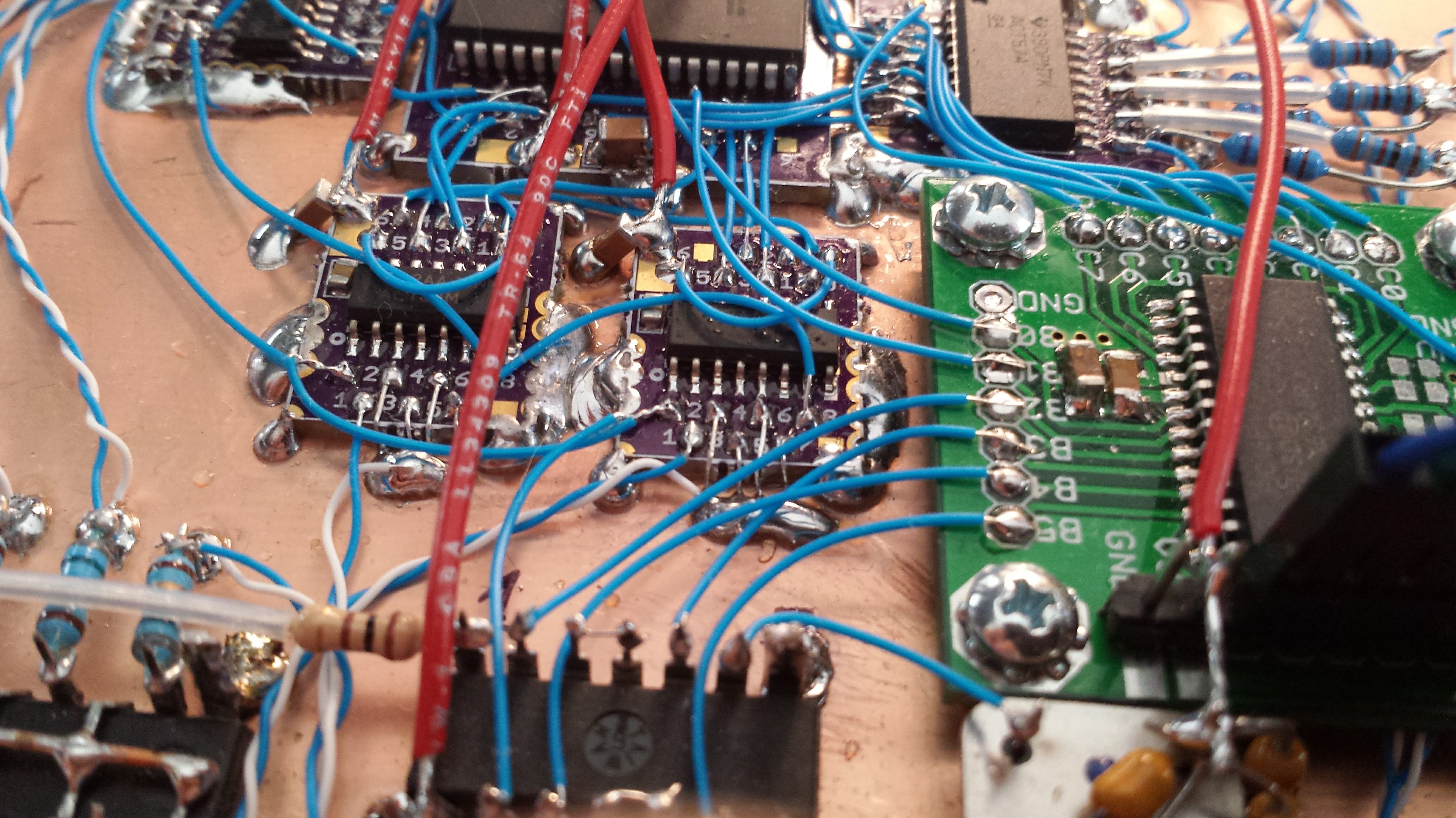
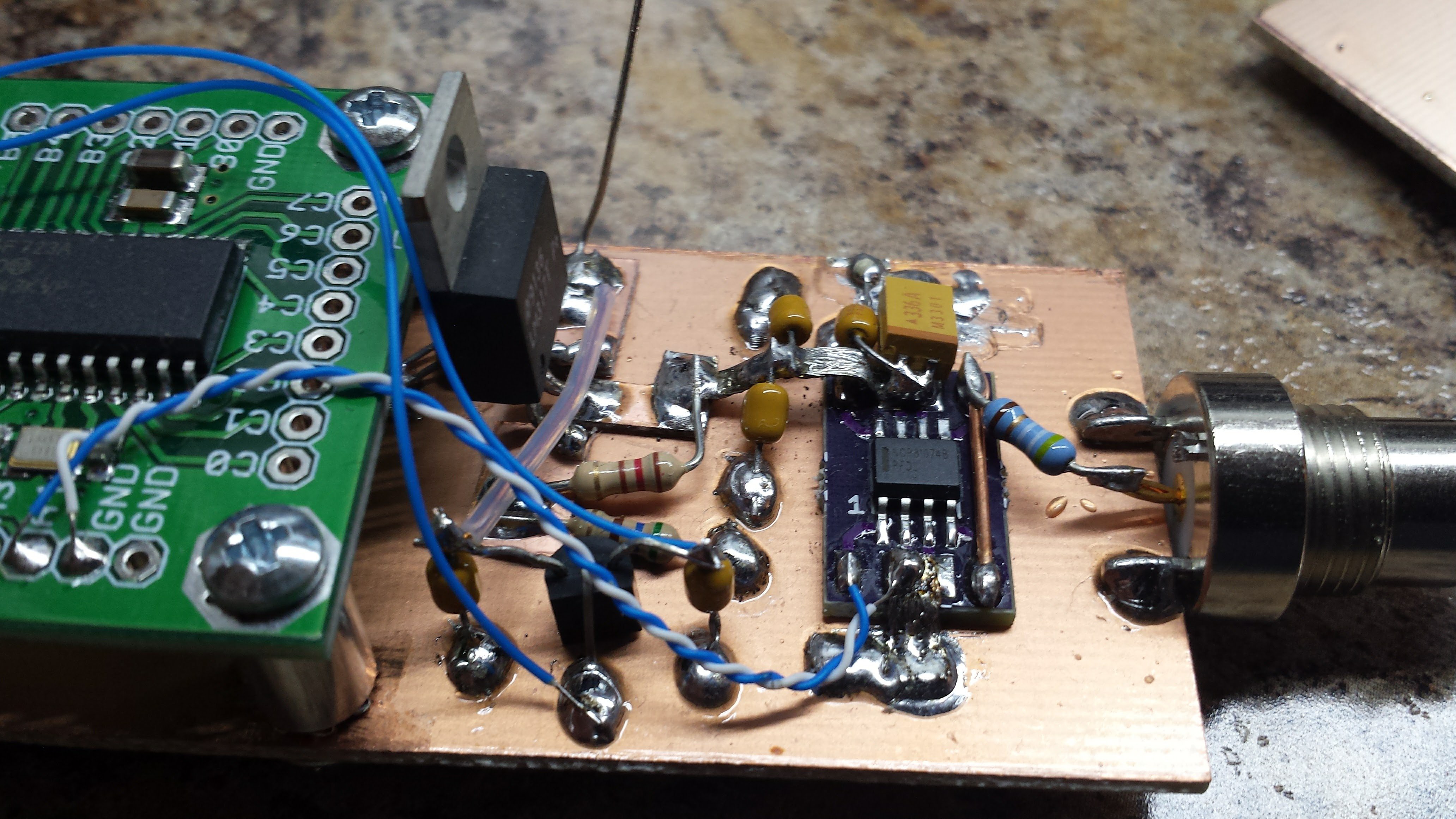
Finally, here's a completely unrelated board that shows how easily the original adapters mix with more traditional prototyping.
Discussions
Become a Hackaday.io Member
Create an account to leave a comment. Already have an account? Log In.