 Daniel Grießhaber
On v0.1 of the Boards, I used the extra SPI interface of the ESP8266-12E Modules to still have enough Pins for the Buttons and other I/O. I also used the "User" and "Flash" Buttons in the same way the NodeMCU did and expected them to not be usable in any other way.
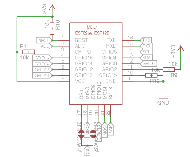
This was the pin mapping of the first version
As it turns out there are quite a few problems with this.
Firstly, the extra SPI Interface on the bottom of the symbol that I wanted to use for the microSD card is actually already connected to the external Flash Chip used to store the executable code for the ESP. Secondly, not only are the SPI pins in use, but the bottom pins are all in use, because the Flash is actually connected via an SDIO interface. As it turns out, Pin 10 (that is connected to the "Right" button is actually already used as a clock signal for the SDIO. This means that when the button is pressed, the clock is held low and the ESP gets stuck because it cant fetch anymore data from the flash.
However, of course the ESP does offer another SPI Interface. This one is mapped to the pins 12-15 in the following manner:
| pin | function |
| 12 | MISO |
| 13 | MOSI |
| 14 | SCK |
| 15 | CS |
So I had to reroute all the pins from the micro SD to these pins, which means I lost all other buttons (Left, Up and Down) that were connected on these pins, so the net problem was: how can I gain some more I/O pins from the ESP?
Well, it turns out that the USER Button that I copied from the NodeMCU schematic is already designed as general purpose input, so I could use it for one function, say Left (I initially thought that the FLASH and USER button were there to switch between flashing and running mode).
Next there was the flash button. it is connected to GPIO2 and pulls it low when pressed. GPIO2 is also connected via a pull-up to VDD. This is needed during boot. If GPIO2 is high during boot, it enters the normal run-mode and executes the user program, if GPIO2 is held low, it enters flash-mode. This check only happens during boot immediately after power-on. However after the chip booted, this pin can be used as a normal GPIO pin. This means that the FLAH-Button can also be repurposed as a normal button. The same principle is true for GPIO0. It also influences the boot behaviour, but after booting, it can be used as a normal GPIO. This means that there are now 2 more usable GPIO pins and I can connect 3 Buttons in total (GPIO16, GPIO2 and GPIO0).
In the v0.1 of the board I had 4 Buttons, in v0.2 there are only 3. The only way I can think of adding another Button would be to replace the I2C Display with an SPI one, which would free SCK and SCL (GPIO4 and GPIO5) but would require one new slave select pin. Still, we would end up with one more pin.
Another way would be to use some diodes and encode the buttons on the 3 available GPIOs as a binary input, which would make it possible to attach (2 ^ 3) - 1 = 7 Buttons in total, however I don't like the fact that pressing multiple buttons then is the same as pressing another button.
The v0.2 Board are ordered and I test how the interface turns out with 3 Buttons (one button needs to have two functions for enter/back which could be done with long clicks). If the UI is not really usable with only 3 Buttons I can evaluate the two options above.
Discussions
Become a Hackaday.io Member
Create an account to leave a comment. Already have an account? Log In.