 Erik Piehl
Update 2016-09-26: SD card access now works
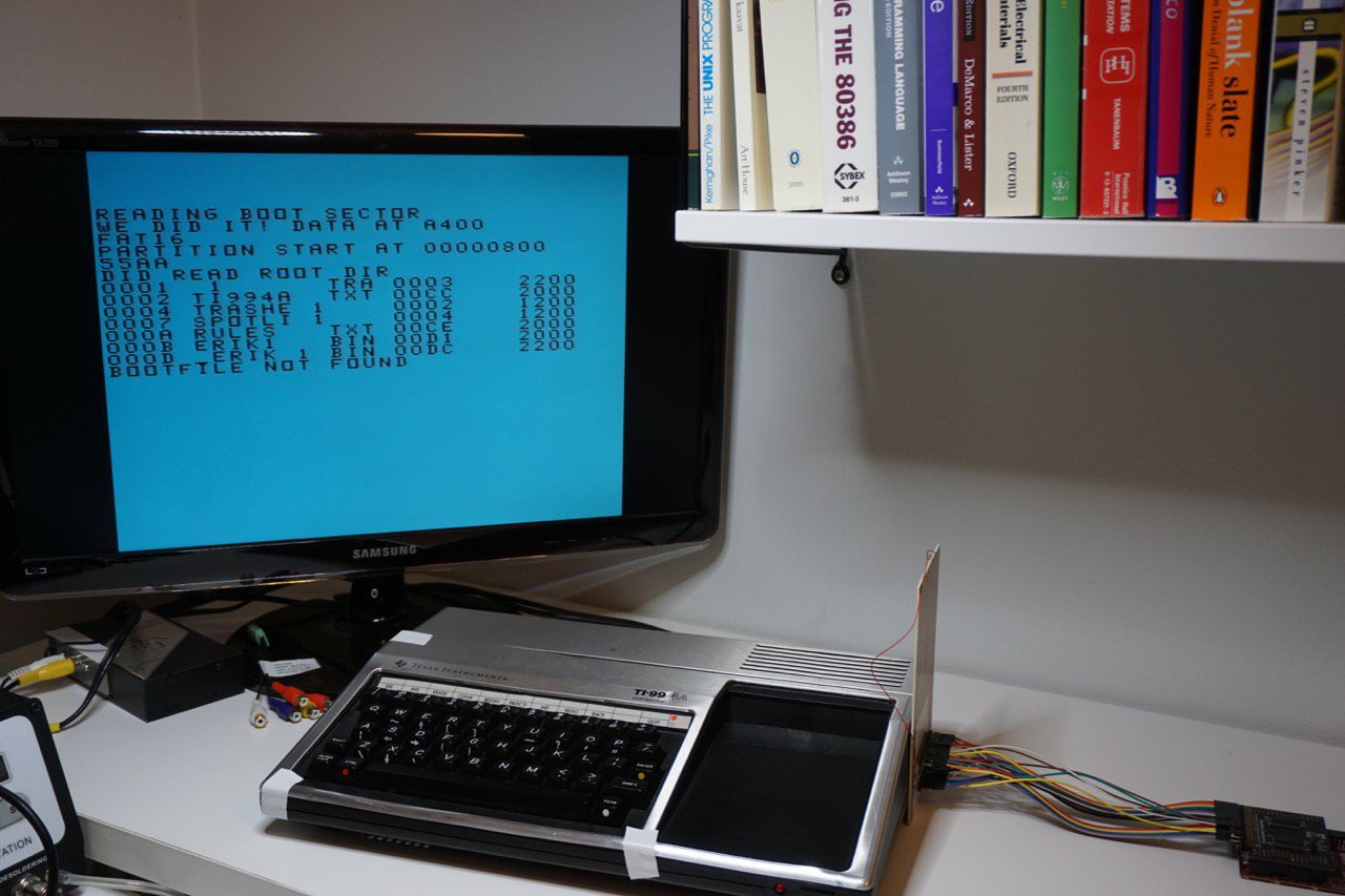
This is one of the first runs of my memory dumper "cartridge" reading data off SD card. The code reads the master boot record, then parses the partition table etc and finally reads and shows the contents of the root directory. This code only understands FAT16 partitions, and does not support yet SDHC cards, so it is running of a 2GB regular micro SD card.
Update 2016-09-24: GROMs moved to RAM
So far in this FPGA design I've kept the GROM memory contents stored on the FPGA's block RAMs, emulating ROMs. The ROM contents became initialised as the FPGA was initialised. But that did limit the amount of GROM the design could include and also made it slow to modify GROM contents. So now I set aside a one megabyte region for GROM contents, and using the PC USB loader I can initialise the GROM contents in the external memory.
Below I have XB2.7 suite running on the TI console. This is usually done using a cartridge, housing 512K of ROM and 120K of GROM. Now both are being served by the FPGA - along with the memory extension.
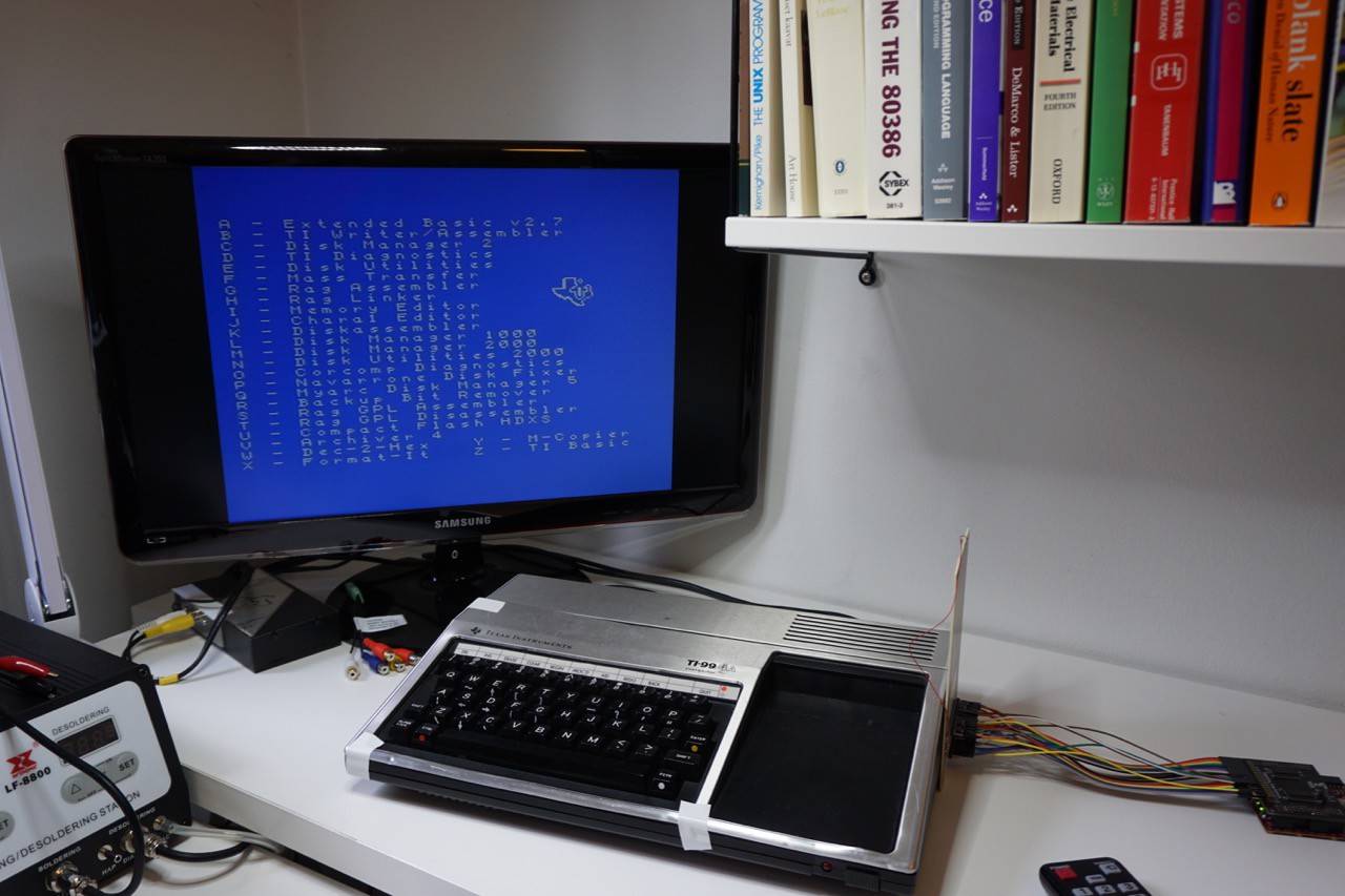
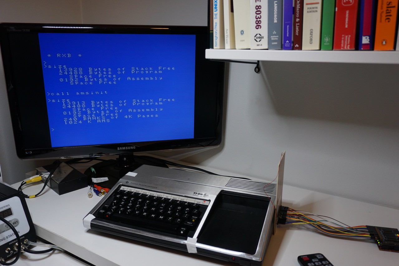
I also tested RXB2015 (another extended Basic), and that worked too. RXB supports SAMS memory, so it was great to see that being detected and working nicely.
Update 2016-09-20: SPI interface and memory dumper
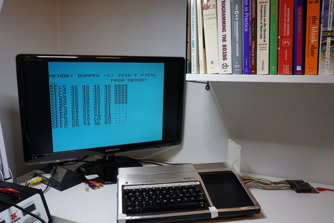
Now there is an SPI interface in place. I adopted it from an earlier design of mine. Testing the SPI requires some driver software, so I put together a simple program to dump memory as a starting point for the SPI testing code (the SPI drives the SD card interface). The memory dumper app includes code to display text on screen and keyboard processing, so the basic building blocks are there. The memory dumper program proved immediately useful, as I finally got the SDRAM interface robustly working. Since PC connectivity is already there, I utilised that for hardware debugging: pressing the period key in the memory dumper copies the values of some hardware registers to memory extension, allowing the PC memory reading capability to reach those values without having to modify the FPGA. The memory dumper itself is written in TMS9900 assembly language and runs in the cartridge memory space (address range 6000..7FFF).
Update 2016-09-04: PC connectivity
In a hobby project like this one, I usually want to build things in an incremental fashion, one small step at a time. So far the project has advanced pretty nicely by just going after the low hanging fruit - basically implementing more or less existing functionality in the FPGA (existing as in RAM extension, cartridge emulation etc.).
Sometimes the small steps just are not possible. For me it came with connectivity. I wanted to finally get to a phase where the modern world would meet the TI to the extent that I could push easily software into it. So I wanted to have PC connectivity - but not your average with a serial port. This project is running on a very high-performance FPGA, something better surely can be done?
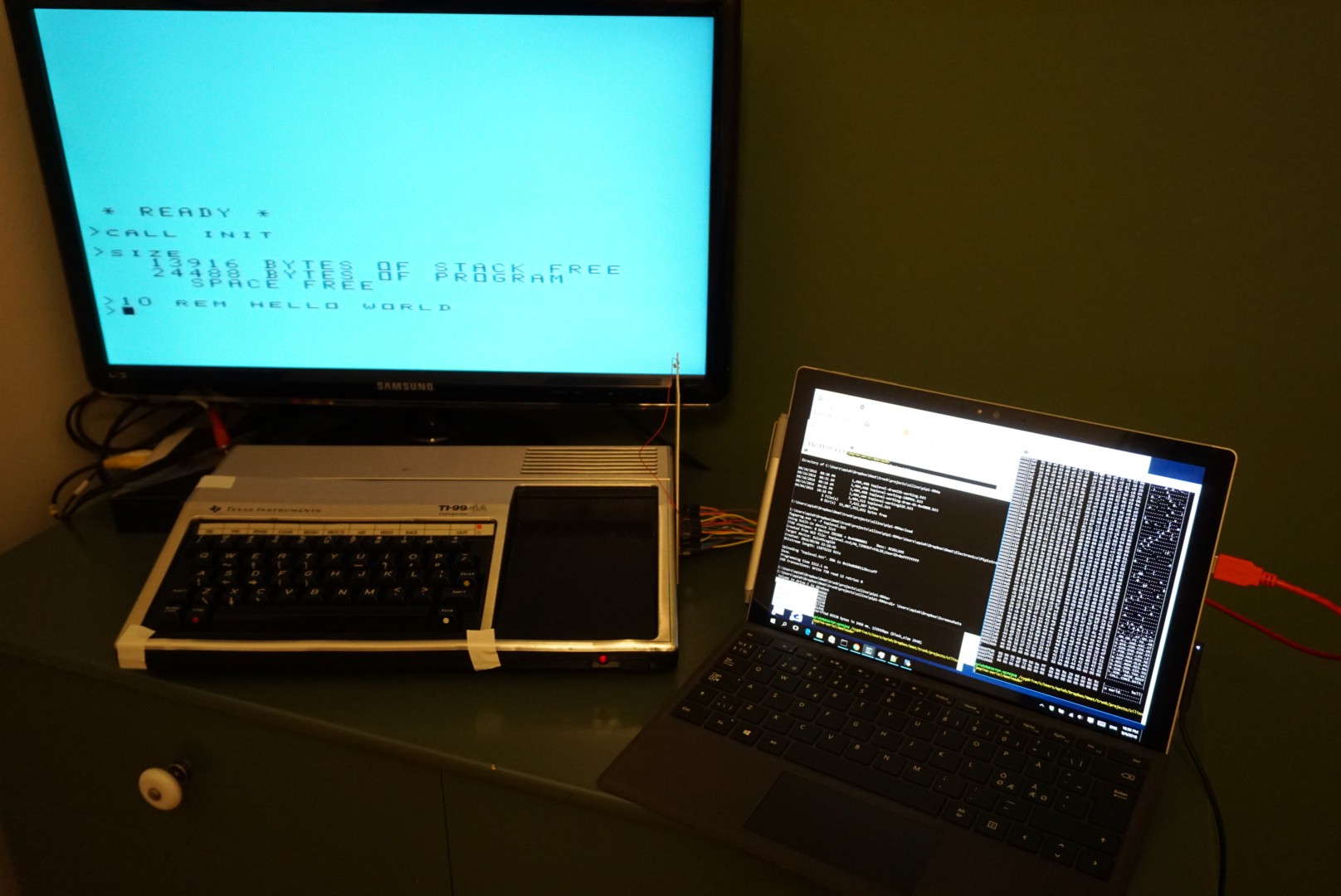
Well I got something much better done. I still have the UART for serial communication, implemented in the FPGA. But it is not the CPU of the TI-99/4A that is communicating with the UART. Instead, there is a hardwired state machine that provides PC access to the memory space concurrently to the TI, basically while the TI is running full speed there is sideband channel that allows a PC to issue commands using the serial port to read and write to memory, without the TI noticing. Serial communication is currently running at 230400 bps, but that could be pushed higher. In practice the serial traffic happens over USB thanks to the FTDI chip on the board.
Alas, that turned out to be more work than I perhaps expected. There were a whole bunch of things to work on, all which were pretty much necessary to complete this feature:
- Define a protocol that is simple enough for a simple state machine to understand, yet something that is useful.
- Build the UART to have the serial receive and transmitter (the UART is talking to the FTDI chip on-board the Pipistrello board). I found a simple UART done in Verilog, so I just needed to interface to it from VHDL and modify it slightly for that purpose. It was the first time for me to do some Verilog programming, so this project became a mixed VHDL and Verilog one.
- Build the state machine which will retrieve received data from the UART, interpret the commands, issue memory read or write commands as appropriate, wait for them to complete, and then send responses back to the host PC. I wanted things to be efficient, so the state machine supports block memory transfers to and from the PC, via an auto incrementing address counter and an auto decrementing transfer length register. This is not hard, but adds to the testing work.
- Build a 2nd state machine to interface to the SDRAM controller's other memory port, so that the memory operations actually go to RAM.
- Modify memory paging so that cartridge ROM contents are fetched from SDRAM instead of block RAM (emulating ROM) in the FPGA. While at it I added support for 128 memory pages, 8K each. So now one megabyte region of the external memory serves as a paged cartridge area. The TI CPU can access this memory at 6000..7FFF. Now thanks to the PC interface, the PC can load any cartridge ROM there. This will make software development cycles very fast.
- Write an application for the PC to communicate with the TI (or rather the memory controller state machine). I wrote that in C under cygwin in a unixy fashion. I tend to mix development of a project over multiple machines (Macs, Windows and Linux machines - it is just me) so having something that is close cross platform is always good.
- Debug all of the above.
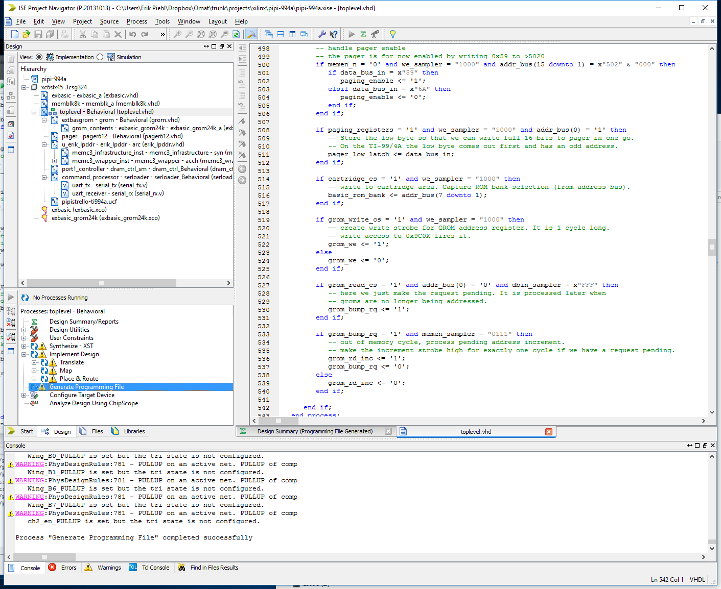
Adding the above also mean that the Xilinx ISE project became somewhat more complex as there are now more functional blocks.
Since there were quite a few steps involved, I decided to approach this in a simplified way - I built a test system on another FPGA board for this (Pepino board), so that I could test the state machines and memory accesses in isolation from the TI. The Pepino has a SRAM chip on it, so that simplified things, as I did not have to deal with the Xilinx memory controller block. This approach of using another board worked well, and also allowed me to focus on the task at hand instead of letting the TI lure me to try things out before they were quite ready...
A somewhat unexpected side benefit of doing the PC communication step was that it allowed me to find a bug I had in the memory interface (from TI to memory extension). I thought I had bug with memory writes, since it seemed that sometimes memory got corrupted. As I was now able to load cartridge images to memory, it allowed me to test memory reads in isolation (basically load a game cartridge ROM from PC to the SDRAM memory and try running it - the game will only read the memory - especially since the FPGA prevents memory writes to cartridge port area as writes are used for bank selection). It turned out that reads did not always work - the games would not run properly. Once I knew that, I tried just giving the memory interface some more time for the address bus to settle before initiating a read - and it worked!
Update 2016-08-26: Simplified version
Finally got the FPGA to do it all. The multi-board solution explained below is now gone, all of those functions are now done with the FPGA. Somewhat unusually the functions typically done by a cartridge are done by the FPGA too, it now has the functionality of the Extended basic cartridge builtin: 12K of ROM and 24K of GROM. In addition there is the SDRAM controller and memory paging system, which supports 16384 pages of 4096 bytes each, to get to 64 megabytes. The paging system (and the entire DRAM system) needs more testing though.
Original project description
The picture with comments hopefully describes the highlights of how this mess of wires is working. Eventually this will get simplified, as I move pieces of functionality from the other devices to the FPGA board. So the final goal of this project is to end up with only the FPGA board, while having more features than the current multi-board setup has.
I first implemented the 32K memory expansion using the FPGA's block RAM. This is a huge FPGA, there is plenty more memory on-chip (over 200K bytes). On the board there is an additional SDRAM chip with a capacity of 64MB, so there is plenty more here to work with... This project (or hack rather) is still in its infancy, my intention is to go much further with the FPGA.
Going to LPDDR SDRAM and Xilinx MCB
After the first iteration of work I started to look into enabling the LPDDR SDRAM, and finally got it pretty much working last night 2016-08-18. This was harder than it should be, because there are not many good examples on how to use the Xilinx on-chip Memory Controller Block from VHDL, especially on this specific board. The MCB is a mean beast - I now have it running at pretty much full speed to my understanding, although I am limited by access through 32-bit ports at 100MHz, so I "only" have a peak bandwidth of 400 Megabytes per second. The MCB sports up to 64-bit wide ports, and it offers up to 6-ports with a choice of scheduling algorithms.
From 8 to 32 bits - what about 16-bit words?
32-bits width is actually the minimum width of the memory controller ports, so to support the TI's external 8-bit bus I had to write extra VHDL code to perform writes with appropriate byte enables and for reads I needed to add a multiplexer to pick up the appropriate byte. Adding those things is trivial compared to controlling the memory controller itself. It is designed for high bandwidth burst mode operation (which is very cool but for simple stuff like this one it is overkill - at least for now). At the end it turned out that operating the controller is not hard, but one needs a state machine to write data and commands to the FIFOs of the memory controller. For reads one needs to first issue a read command for a one word burst, wait for it to go and fetch the 32-bit word, then read it from the FIFO and finally feed it to the bus of the TI.
In my implementation I finally added a separate 32-bit latch to capture the memory word, so that individual bytes can be accessed without additional reads. This is important since the TI's external bus seems to assert DBIN (memory read signal) and MEMEN (memory access enable) in the beginning of a 16-bit bus cycle, i.e. only once for the two bytes that will be transferred. The TMS9900 seems to address memory always as 16-bit words - for byte access it does a read-modify-write cycle - external logic in the console then breaks the 16-bit transfer into two 8-bit transfers. All this means that mid cycle A0 (or A15 in TI parlance, the least significant address bit) will change without any changes in DBIN or MEMEN. [Also the console circuitry seems to create glitches that are visible on the address bus in the very beginning of a memory cycle. The VHDL code attempts to steer clear from those by sampling DBIN and WE (write enable) over four 100MHz clock cycles before asserting an internal memory operation request.] Since my implementation does a single 32-bit memory read for the first byte wide memory read, it will have the other byte of a 16-bit memory access already in the 32-bit latch and thus available.
From 32K to 64M
I am currently in the process of incorporating a "Super AMS" compatible memory paging unit into the design. This is right now work in progress. I had a 74LS612 compatible design already for another project FPGA99, but that needed some changes (such as extending the page registers from 8 bits to 14 bits to cover for a 64 megabyte address space). I will probably make the page registers visible for software through two different ways, one that is "Super AMS" compatible (limited to one 1 megabyte) and another one that is extended to be able to address the whole address space of 64 megabytes. The way I think this should be done is by having the Super AMS style access only modify the bottom 8 bits of page registers, maintaining the previous values at the higher order bits.
Why 64 megabytes?
One might ask why it would be a good idea to have 64 megabytes on the TI? After all, the original console memory expansion was limited to 32K bytes. Also, the external memory bandwidth of the TI-99/4A is very slow, only 1 megabyte/second. So just touching the entire 64 megs of memory by the CPU would take a good while - several minutes in practice.
The answer is simple of course - the FPGA board has 64 megs, so all of that must be available :). A somewhat more intelligent answer is that the FPGA board also has a SD card slot. My intention is to make the FPGA load ROM content (both TI GROMs and cartridge ROMs) from the SD card to DRAM. For example if I allocate 8 megabytes for ROMs and another 8 megabytes for GROMs, I could have up to a thousand cartridges loaded simultaneously, that would probably be close to the entire software library for the machine. Normally you would not be able to put paged RAM, GROM and ROM content into the same memory chip, but the FPGA can easily manage the necessary address manipulation. It could also do the loading from the SD card at a great speed, far faster than TI could do via software, so it would effectively create a DMA based memory loader. The transfer speed should easily exceed 1 megabyte per second, so it would not take long to load 16 megs worth of content.
Getting Extended BASIC to run
TI in their infinite wisdom did not enable the built-in Basic ROM to access memory with PEEK or POKE style commands - or to even use the memory expansion. Thus in order to test the memory expansion, TI Extend BASIC cartridge is needed. I did not have it, so this project started as a hack on a game module to make it extended basic. I crudely soldered a ZIF socket for a memory chip to have the ROM memory. That's not enough though, as the extended BASIC has 12K of ROM while a normal cartridge directly only has 8K address space available. So you need to implement memory paging. For me the easiest way to add that logic was to connect my own "SD Processor" board (featuring NXP LPC1343 MCU with USB, SD card socket, and Xilinx 95144XL CPLD for glue logic). In this circuit only the CPLD is slightly used, to implement the memory page latch and chip select logic.
But even that is not enough, the extended BASIC cartridge also included 4*6K=24K of GROM capacity. The GROM's were TI's proprietary memory devices with 6K capacity each. In this system that part is implemented with LPC1114FBD48/302 micro controller - soldered on a 48-pin LQFP breakout board. The cool thing about that its firmware is programmed with a Raspberry PI - making that part of this mess "Internet enabled" :) Thus it is easy to update the firmware. I'm pretty happy with the firmware even if it is a quick-and-dirty hack, as it makes 30K of the 32K flash memory of the micro controller available as GROM, making it possible to pack the contents of 5 GROM chips on-chip. In other words, the GROM emulation code (with some serial debugging stuff) fits into the remaining 2K of the flash memory.