 hkdcsf
Objectives:
- receiving date and time from the DCF77 transmitter, decoding it, displaying it on a 128x64 pixel dotmatrix display
- receiving UTC from GPS satellites with a GPS module, displaying it on a 128x64 pixel dotmatrix display
- stand-alone date and time clock based on a real time clock (if radio signal reception is not possible)
- measuring and displaying temperature
- measuring and displaying battery voltage
- displaying SW version information
- simple menu system for configuration
- alarm function
- beep sound on button press
HW block diagram
On the picture below You can see the HW block diagram.
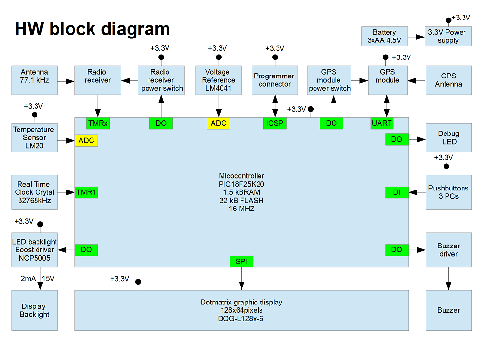
I built the project around a PIC microcontroller. The goal was during the micro selection is to have a low power consumption but yet powerful enough controller to decode the DCF77 and GPS signals and to drive the display. I also choose a type which I familiar with.
The display is a chip-on-glass type which can be powered from 3.3V. It can be controlled via a simple SPI protocol. Another advantage is that no mounting required, it can be simply soldered on the PCB, but i will use a header adapter so the display can be changed easily.
The LED backlight is powered with an NCP5005 boost driver. The clock will be running from 3 AA batteries. To decrease the power consumption the SW has to have some intelligence: dimming, or even switch off the backlight at certain time of the day.
I used a small 32768 kHz real time clock crystal, so the clock can remain relatively punctual even when no DCF77 or GPS reception is possible.
For temperature measurement an analog LM20 sensor is used.
In order to measure the output of the temperature sensor and the battery voltage accurately an LM4041 voltage reference is used.
Programming and debugging is performed with a PICkit3 programmer, so a header adapter is connected to the ICSP of the micro as programmer connector.
For powering the whole circuit 3 AA battery is used and a very low drop 3.3V voltage regulator.
For easier debugging and for measurement purpose during the development a red LED is directly connected to a micro output with a series resistor.
To be able to operate the menu and set the date and time 3 taktile type push buttons is connected to 3 microcontroller inputs with pull-up resistors.
A TDK PS1720P02 piezo buzzer is used for generating a sound signal when a button is pressed and for the alarm clock functionality.
For UTC reception from a GPS satellite a PmodGPS module is used from Digilent.
For exact time and date reception a DCF 77 receiver module with digital output is used from Conrad electronics.
Schematic
On the picture below You can see the schematic of my project.

I tried to isolate the main blocks therefore I added a grey dashed line frame around them to easily identify which block is doing what.
I used Eagle 6.6.0 PCB editor for creating the schematic.
System design: GPS signal processing
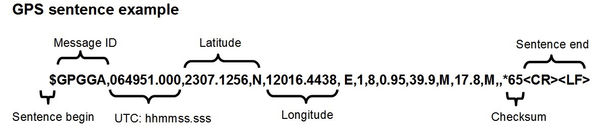
What is the interface protocol of the PmodGPS module?
According to the data sheet "The PmodGPS uses sentences
based on National Marine Electronics Association (NMEA) protocols for data
output. Each NMEA message begins with a '$' dollar sign. The next five
characters are the talker ID and the arrival alarm.
The
PmodGPS talker ID is 'GP' and the arrival alarm is the specific sentence output
descriptor. Individual comma separated data fields follow these five characters.
After the data fields there is an asterisk followed by a checksum. Each sentence
should end with <CR><LF>. <CR> is the carriage return its ASCII
value is 13, <LF> is the line feed character its ASCII value is 10.
You can see an example GPS sentence on the picture
below:
 Some other examples:
$GPGGA,064951.000,2307.1256,N,12016.4438,
E,1,8,0.95,39.9,M,17.8,M,,*65<CR><LF>
$GPRMC,064951.000,A,2307.1256,N,12016.4438,E,0.03,165.48,260406,3.05,W,A*55<CR><LF>
How we receive
these GPS sentences?
Each character in the GPS
sentence corresponds to one UART (Universal Asynchronous Receiver Transmitter)
byte. The data value of this byte is equals to the corresponding ASCII character
representation value.
The PmodGPS uses UART protocol
for data transmission and reception. The interface operates at a baud rate of
9.6 kBaud, 8data bits, no parity, and with single stop bits. This PIC does not have
a DMA peripheral, therefore we are using an interrupt on each UART byte
reception to save the received UART byte into a buffer for further
processing.
How we process the GPS sentences?
So we have a large buffer in the memory full of received UART bytes. How
we determine where is the beginning of a GPS sentence in this buffer? In the
UART reception interrupt we also counts how many <LF> character are put in
the buffer. If we have more than 2 <LF> than a full GPS sentence is surely
in the buffer. In this case we zero the buffer counter and stop further UART
byte reception until we processed the last received GPS sentence.
Using the $ sign and the <CR><LF> character
pair we can search for the beginning and the end of the GPS sentence.
How we check
the validity of the GPS sentences?
Checksum
validation:
The checksum is simply the bitwise xor of
the character values in the GPS sentence between the $ and the * sign, including
the commas too. This checksum is calculated by the PmodGPS module, and inserted
in the GPS sentence between the * and the <CR><LF> characters. As a
sentence validation we check whether the received checksum is the same what we
calculate from the received characters between the $ and * sign.
Sentence format validation:
When we
extract the UTC, latitude and longitude information from the GPS sentence we
also checking:
- whether in the character positions where a ',' or '.' character should be we really received one of these characters
- whether in the character positions where a number should be we really received a number
- whether in the character positions where a 'N', 'S', 'E' or W' character should be we really received one of these characters
How we extract the time from the
sentences?
If we received a valid sentence we check
the message ID of it.
Sentences with GPGGA or GPRMC are
containing the UTC information.
Therefore if we receive
such a sentence we extract the characters between the first and second comma in
the sentence. These characters are the UTC data.
How we convert UTC
to our local time?
My local time is the CET Central
European Time. This means that the time in my region is UTC+01:00 at winter and
UTC+02:00 at summer CEST (Central European Summer Time).
The changing between winter to summer time occurs at 01:00 o'clock on the
last Sunday of March.
The changing between summer to
winter time occurs at 01:00 o'clock on the last Sunday of October.
Therefore I have written a small function which computes
based on the local date whether we have summer or winter time.
This function is called each time when we receive the UTC
from the GPS module, the +01:00 or +02:00 offset to the UTC is determined
according to the summer or winter time and the time on the LCD screen is updated
accordingly.
How we synchronize our local clock
precisely to the GPS clock?
The PmodGPS module has a 1PPS output signal. You can see the
shape of this signal on the picture below.
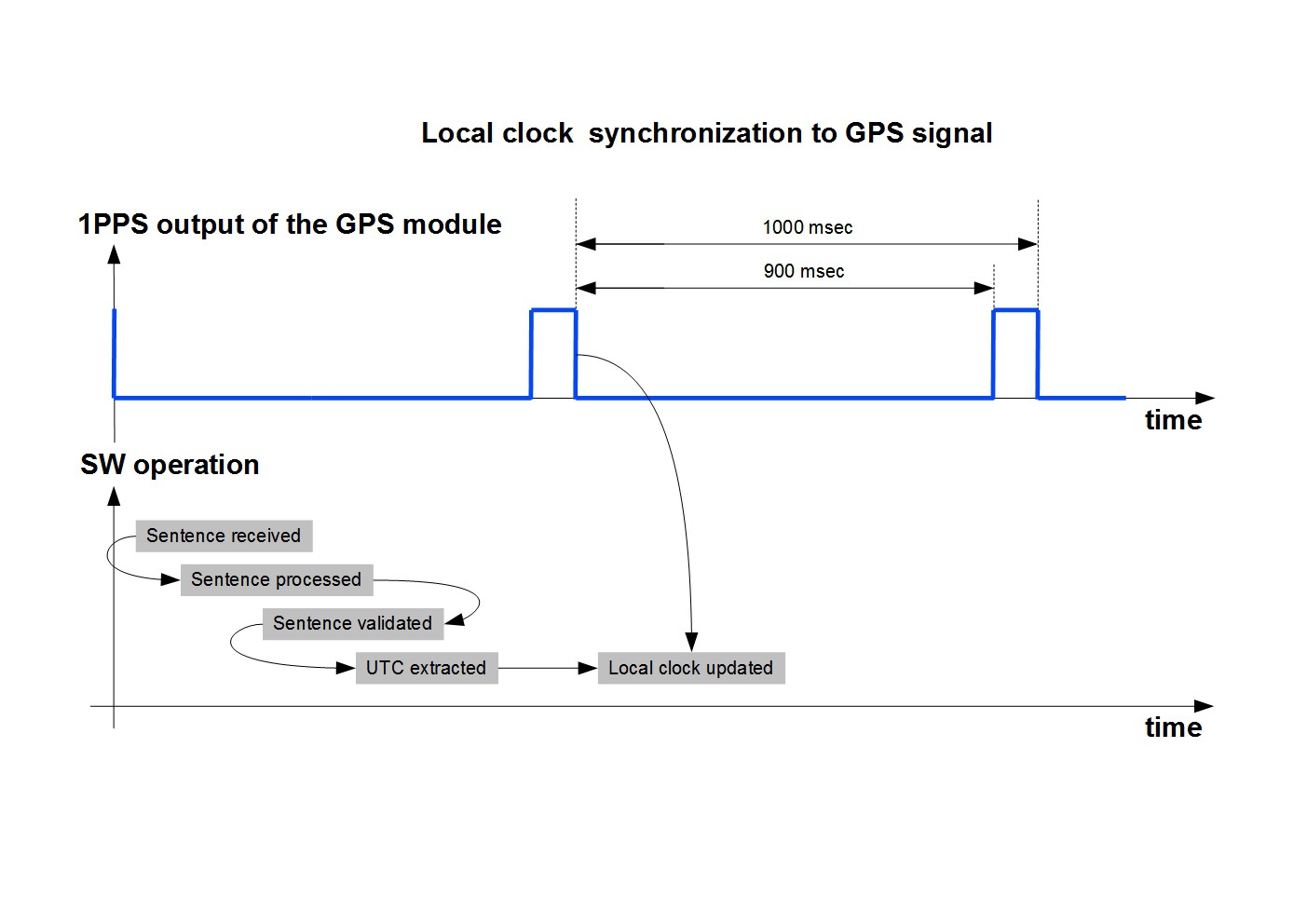
Upon reception of a valid GPS sentence via UART containing the
UTC information we are updating our local clock on the falling edge of the 1PPS
signal of course with the second counter incremented. You can see this
synchronization method on the picture above.
GPS 1PPS signal and UTC reception video
On the video below You can see on the oscilloscope how the GPS 1PPS signal waveform looks like. You can also see how the clock is synchronizing to the GPS signal.
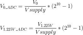
System design: power supply voltage measurement
How to calculate the power supply voltage if you have a precision reference voltage source connected to one of the ADC inputs?
In case of a 10 bit ADC You can calculate the ADC conversion result in general with the following formula:
In our case the ADC reference voltage is connected to the power supply, and we have an 1.225V reference (LM4041), which gives:
Solving this equation to Vsupply gives:
Since this micro has only an integer arithmetic, and we are interested only in the last two digit after the decimal point we multiply this equation with 100 which gives:
This equation was implemented in the code. I simply divide the constant 125317 with the ADC conversion result and get the Supply voltage multiplied by 100. Write this result to the LCD display with a decimal point between the 2nd and 3rd digit.
System design: DCF77 signal processing
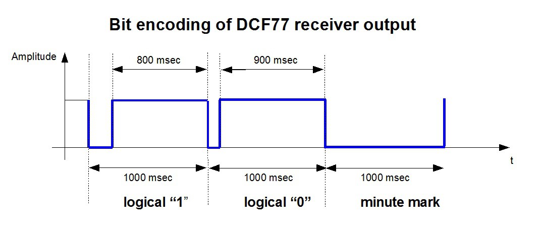
How the bits are encoded?
On
the picture below You can see the bit encoding at the output of the
DCF77 receiver module. A 100msec length active low pulse represents the
logical '0', a 200msec one the logical '1'.
What information is sent by the transmitter?
On
this quite informative picture below You can see what kind of
information is sent by the transmitter during a 60 second time frame. We
are using the 'Minute', 'Hour', 'Calendar day', 'Day of week', 'Month',
'Year' datas. These are transmitted in BCD (binary coded decimal)
format. P1, P2 and P3 are parity bits. There are other bits also for
whether forecast, daylight saving time notification etc. these fields
are currently not used by this project.

Picture source: ptb.de
How the bits are decoded by the PIC?
As
You can see on the schematic: the output of the DCF77 receiver module is
connected to two capture compare inputs of the microcontroller (CCP1 and
CCP2). CCP1 reacts on falling edges, CCP2 on rising edges. We are using a
timer (TIMER3) for measuring the pulse length. If we have a falling
edge an interrupt is triggered which starts TIMER3, on a rising edge an
another interrupt is triggered which reads the value of TIMER3. Based on
this timer value we can measure the elapsed time between the edges an
we can decide whether we had a 100msec or 200msec pulse length, in other
words whether we received a '0' or a '1' bit.
What problems to tackle with the decoding algorithm?
On the scope pictures below You can see the two main problem of the output signal of the DCF77 receiver module:
problem 1:
pulse length variance (jitter). The oscilloscope picture below was taken with
persistence mode on. You can see that the 100msec pulse length varies
from ~90msec to ~120msec:

problem 2: multiple switching during edge transition

Both of these problems can be handled with a 'tolerance window'. With this method we accept a pulse to be a logical '0' if the length is between 66.6 and 141.6 msec and to logical '1' if the length is between 150 and 266 msec. Otherwise we skip the edge transition but resets our timer to 0. The tolerance window beginning and end values (66.6, 141.6, 150 and 266) are determined with oscilloscope measurements of the DCF77 receiver module output.

How to validate the received data?
The following validation methods were applied:
- parity bit checks: whether the received P1, P2, P3 parity bits are the same what we computed from the received data
- range check of received data e.g. whether the received 'Month' value is smaller than 13, etc.
We are updating our local clock and the LCD screen only if these validation checks are succeeded.
How we synchronize our local clock precisely to the DCF77 clock?
This can be handled easily since the DCF77 signal has a minute mark part, as soon as we received the falling edge of this mark we update our local clock with the received time and date information and refresh the LCD content with this new data.
DCF77 signal reception video
On the video below You can see on the oscilloscope how the DCF77 signal waveform looks like. You can also see how the two separate clocks are synchronizing to the DCF77 signal.
System design: menu system
On the picture below the menu system state chart is shown:

Videos about the menu system:
This video shows the operation of the middle part of the state chart above, where the stand-alone clock can be set.
This video shows the operation of the lower part of the state chart above, where the menu settings are demonstrated:
System design: power consumption considerations
This project will run from three AA type batteries, so it is essential to have a low power consumption.
What methods I used to decrease the power consumption?
1. The processors power consumption is proportional with clock speed. Therefore the PIC is running on the slowest possible speed to perform the needed computation tasks. This is currently 1 MHz, which results around 0.5mA current consumption according to the datasheet.
2. low voltage drop stabilizer is used, in order to minimize the power dissipation on the linear regulator
3. LCD background light can be switched off by SW
4. high value pull up resistors used
5. the power supply of the receivers are switchable, so the SW can switch of these main power consumers when the local clock is synchronized to GPS or DCF77. On the picture below You can see how this mechanism works:

System design: temperature measurement
How to calculate the temperature value efficiently and accurately in the SW from the output voltage of the temperature sensor?
I.
According to the datasheet of the LM20 temperature sensor the relation between the temperature (T) and the output voltage of the sensor (Vo) is the following:

It can be seen that the relation between T and Vo is slightly non linear.
I do not want to waste so much computation power of this little PIC micro to exactly calculate the temperature according to this formula. Instead, I calculated what this formula gives at 30°C and at 10°C (most probable temperature operational range). Knowing these values a straight line was fit which goes through these points. The equation of this line is:
 Approximating the temperature with this simplified equation gives a 0.1% error in the 10°C-30°C temperature range which is quite acceptable.
II.
Since we have an 1.225V LM4041 voltage reference connected to one of the ADC pins, we can use this as a reference for temperature measurement ADC conversion. Using this reference instead of the ADC reference (which is the 3.3V power supply of the PIC) has two advantages:
- (i) it is more accurate: LM4041 has +-0.1% max deviation from nominal; TC1108 has +-0.5% typical +-2.5% maximal deviation to nominal
- (ii) more importantly: if the battery voltage drops below 3.3V we still can calculate the temperature accurately
Lets compute Vo by dividing this two equation:
This gives for Vo:
Substituting this formula for Vo into our equation for the temperature gives:
III.
Since this micro has only an integer arithmetic, and we are interested in the last two digit after the decimal point we multiply this equation with 100 which gives:
This equation was implemented in the code for temperature calculation. Divide the ADC conversion result of the temperature sensor with the ADC conversion result of the 1.225V voltage reference, multiply it by 10511 and substract this result from 16002. Write this result to the LCD display with a decimal point between the 2nd and 3rd digit.
Software
In this chapter I will give some information about the software static architecture, software dynamic behavior, and coding.
Coding
The code operating the clock was written in C. For the C code the following naming conventions were used.
Naming conventions:
- each SW unit has a 3 letter unique identifier, eg. GPS, LCC
- this identifier is used in the variable and function names of the SW unit
- the variable type is encoded in the variable name, this is the so called Hungarian notation, which makes the identification of the variable type more easier in the code line where the variable is actually used
Naming of functions:
Lets take an example:
void LCC_v_SendCommand_f(u8_t u8_command_p, u8_t u8_Data2write_p);
This is a function (_f) in SW unit called LCC with void return type (_v_) and with 2 parameters.
Naming of variables:
Lets take an example:
static u8_t L_GPS_u8_Hours = 0u;
This is a local variable (L_) in SW unit called GPS with 8bit unsigned storage class (_u8_).
Software static architecture
On the picture below You can see the software static arhitecture: the software units building up the SW system and the main connection between them. Each SW unit has a 3 letter unique identifier. Below the picture You can check what is the functionaility of these SW units.
I have also displayed the HW-SW interface too: which microcontroller peripherals are used and which HW component it connects to.

BZD:
This SW unit is the BuZzer
Driver. It is responsible for driving the buzzer with a 5 kHz signal
when its interface function is called.
CNV:
This SW unit is
responsible for various data CoNVersions such:
- binary number to BCD,
- BCD to decimal number,
- ASCII number character to decimal number
DCF:
This SW unit is the low
level DCF-77 driver, it:
- handles the TIMER3 timer and CCP peripherals,
- collects into variables the bits received from the DCF77 receiver at each second
- on falling edge it clears TIMER3 on rising edge reads TIMER3 to determine whether '0' bit or a '1' bit is received
- provides interface functiton for switching on and off the power supply of the DCF receiver module
DCP:
This SW unit is the DCF77
Protocol driver, it:
- checks the parity of the received data
- collects the received bits into the corresponding variables
- check the validity of the data: whether the received data and time information is in range e.g. hours are not bigger than 24, etc
- updates the stand alone clock with the received date and time if the checks are passed
GPS:
This SW unit is the GPS
driver, it:
- handles the UART byte receiving interrupts and puts the received UART bytes into a buffer for further processing
- processes the received GPS sentence:
- compares the received and computed GPS sentence checksum
- prepares the last received GPS sentence to be write on the LCD screen
- identifies GGA and RMA GPS sentences
- extract UTC, latitude and longitude information from GPS sentences
- prepares UTC, latitude and longitude information to be write on the LCD screen
- updates the stand alone clock upon reception of a valid UTC information
- provides interface function for switching on and off the power supply of the GPS receiver module
INT:
This SW unit is the
INTerupt driver, it handles:
- the interrupt on RB1, RB4 and RB5 pins upon a button press
- the interrupt rutin of the TIMER1 peripheral used for RTC (Real time clock)
- the UART reception interrupt
- the interrupt on CCP1 and CCP2 pins for DCF77 reception
- it implements delay functions used in other part of the SW
LCC:
This SW unit handles the
LCD Content, on a function call it:
- writes the time: hours, minutes, seconds to the LCD
- writes the date: year, month, days, weekdays to the LCD
- writes the temperature, battery voltage
- draws and clears the radio signal symbol
- draws the receiver selection: DCF or GPS
- clears the screen
- writes build information
- writes the menu content
- draws boot-screen
- writes GPS sentence, UTC, latitude and longitude information
LED:
This SW unit is the LED
driver, on a function call this drivers can switch on or off:
- the debug LED
- the LCD back-light driver
LPD:
This SW unit is the LCD
display low level Protocol Driver:
- on a function call it can send commands and data to the LCD display via SPI
- it handles the MSSP serial peripheral and some GPIO pins to send SPI messages
SCD:
This SW unit is the
Stand-alone Clock Driver. It is responsible for running a local clock
based on the local 32768kHz crystal.
- it computes the time and date
- it handles the leap-years
- provides a function which can update the local clock and date on reception of a GPS or DCF signal
- it provides functions to increment and decrement the time and date to set the exact time and date of the local clock with the push buttons
- it calculates the UTC offset during winter (CET) and summer (CEST) time
TIM:
This SW unit orchestrates
the operation of all the other SW units. It is The Interrupt Manager.
- it handles the alarm functionality of the clock
- updates the LCD screen content according to the current state of the state machine
TMD:
This SW unit is the
Temperature Measurement Driver. It gets the temperature
and voltage reference ADC values from the VMD driver and computes the
temperature according to the sensor characteristics.
UAT:
This SW unit is the UART
Driver.
- It handles the EUSART peripheral of the micro controller, initialize the transmission and reception to the required format of the GPS module.
- It provides interface function for sending an UART byte to the GPS module.
VMD:
This SW unit is the
Voltage Measurement Driver. It handles:
- the analog to digital converter peripheral module o the micro-controller.
- the measurement of the battery voltage.
- Provides function for getting the ADC data.
Software dynamic behavior
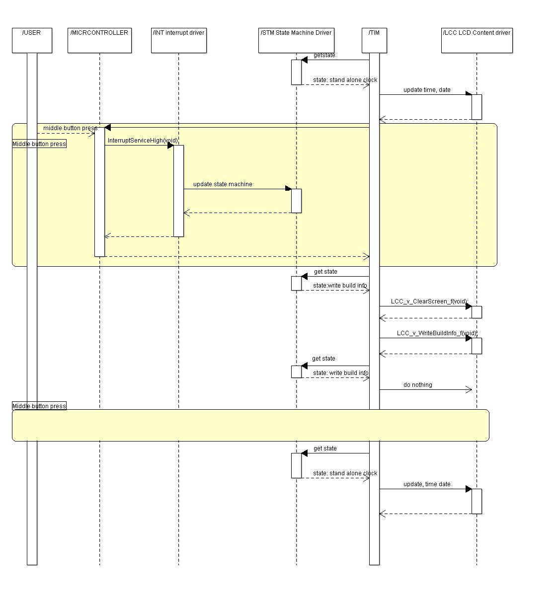
On the sequence diagram below, you can see what happens between the SW units when You push the middle button of the clock to displays the SW version information.
PCB design
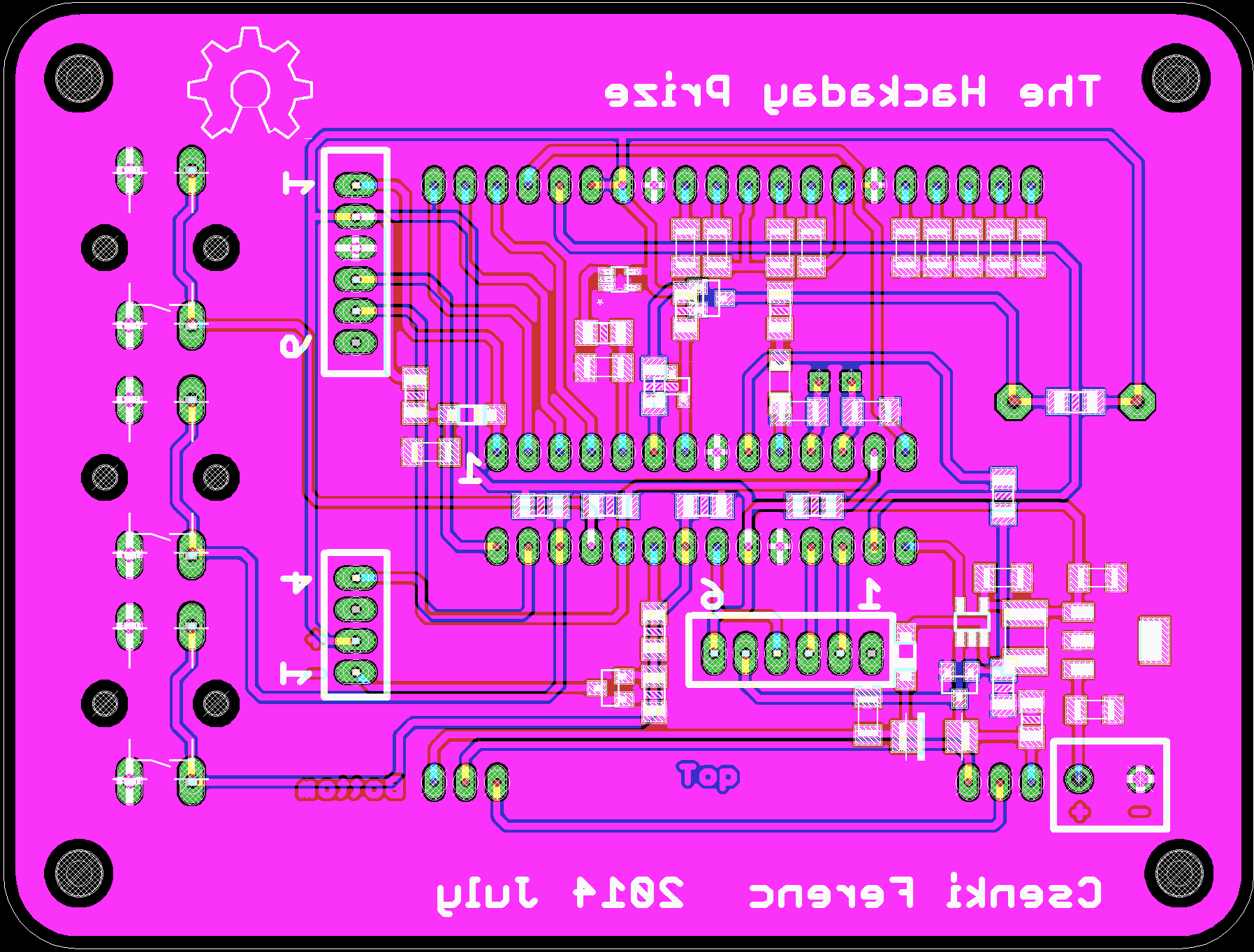
The goal was during the PCB design is to have an ergonomic placement of the buttons and the LCD display and to to fit the PCB into a Deltron 479-0160 enclosure. The PCB will be the top of the enclosure with the buttons and the LCD display on the Top side of the PCB board. I used only two layers. I was using the free version of the Eagle PCB designer 6.6.0. PCBs with blue and with a red solder masks are manufactured.
Tools used
In this chapter the open-source licenses and permissions as well as any applicable third-party licenses/restrictions are documented.
I used only free tools for creating the design and documentation.
Documentation, drawings: Open office 4
Schematic and PCB design: EAGLE 6
Programming: C language, C99
Source file editing: Eclipse
Code compilation: MPLAB IDE v8.84
Equation editing: free LATEX
Drawings: yED 3.11, ArgoUML
System design and status summary
- receiving date and time from the DCF77 transmitter, decoding it, displaying it on a 128x64 pixel dotmatrix display - this functionality is working
- receiving UTC from GPS satellites with a GPS module, displaying it on a 128x64 pixel dotmatrix display - this functionality is working
- stand-alone date and time clock based on a real time clock (if radio signal reception is not possible) - this functionality is working
- measuring and displaying temperature - this functionality is working
- measuring and displaying battery voltage - this functionality is working
- displaying SW version information - this functionality is working
- simple menu system for configuration - this functionality is working
- alarm function - this functionality is working
- beep sound on button press - this functionality is working