0%
0%
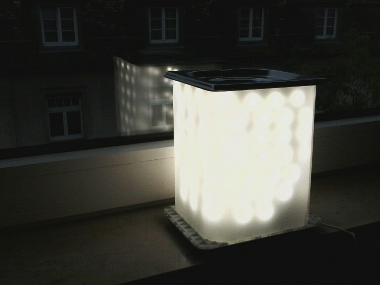
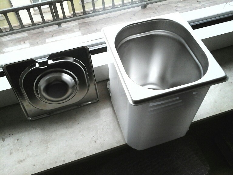
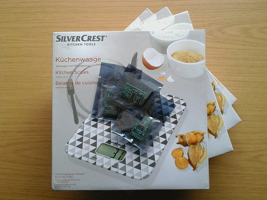
automated gardening - reservoir infrastructure
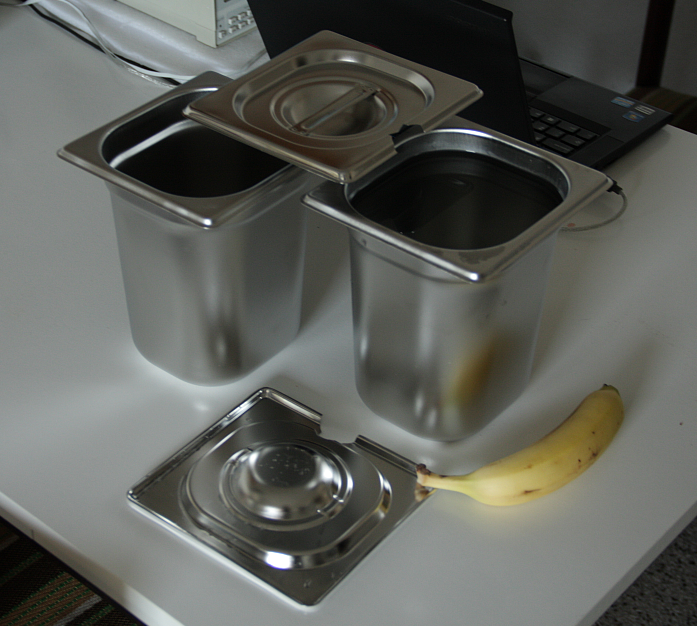
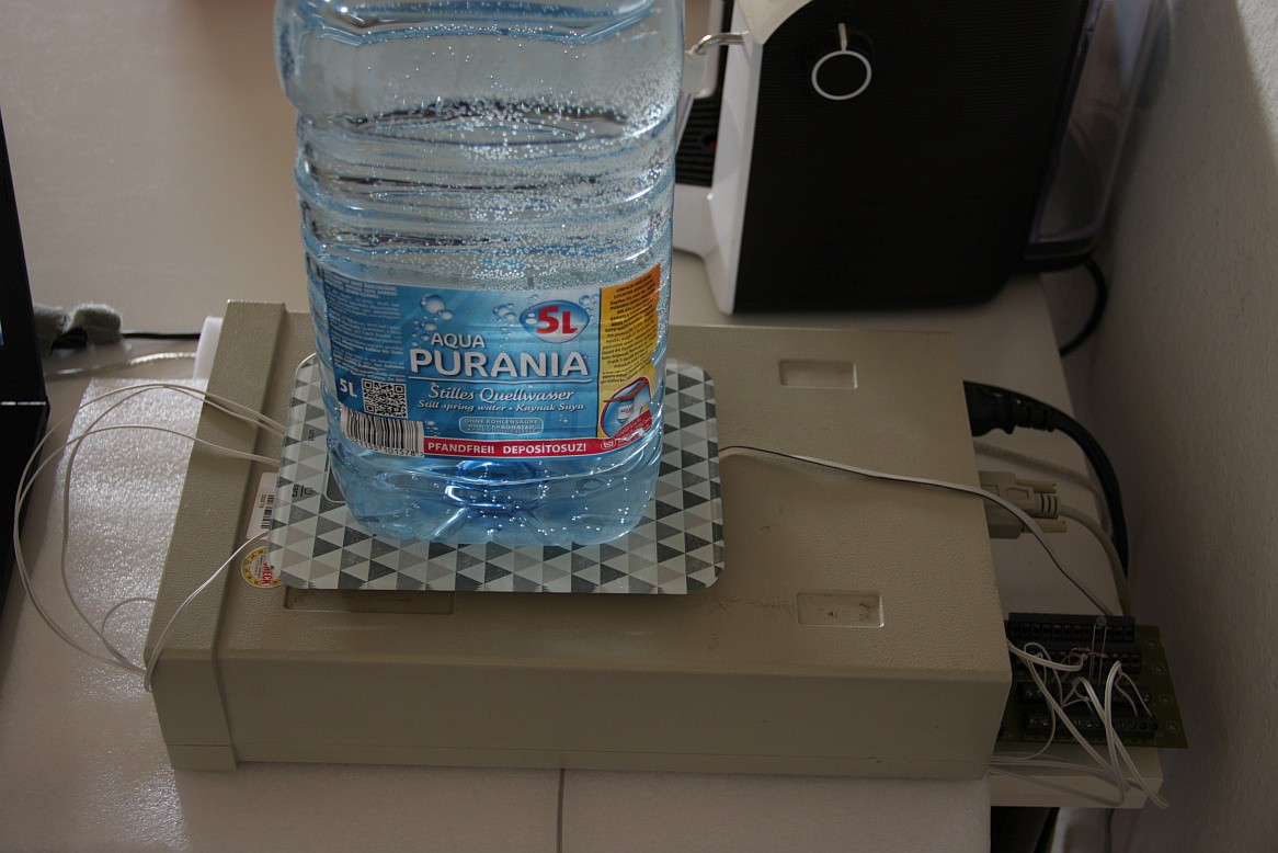
Building Reservoirs and Weighing Water for level gauging and flow metering.
 helge
helgeBecome a Hackaday.io member
Already have an account? Log in.
Just one more thing
To make the experience fit your profile, pick a username and tell us what interests you.
Pick an awesome username
hackaday.io/
Your profile's URL: hackaday.io/username. Max 25 alphanumeric characters.
Pick a few interests
Projects that share your interests
People that share your interests
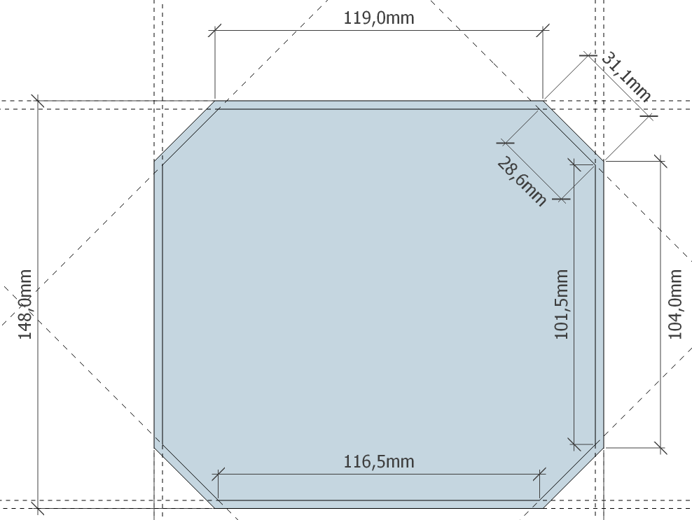
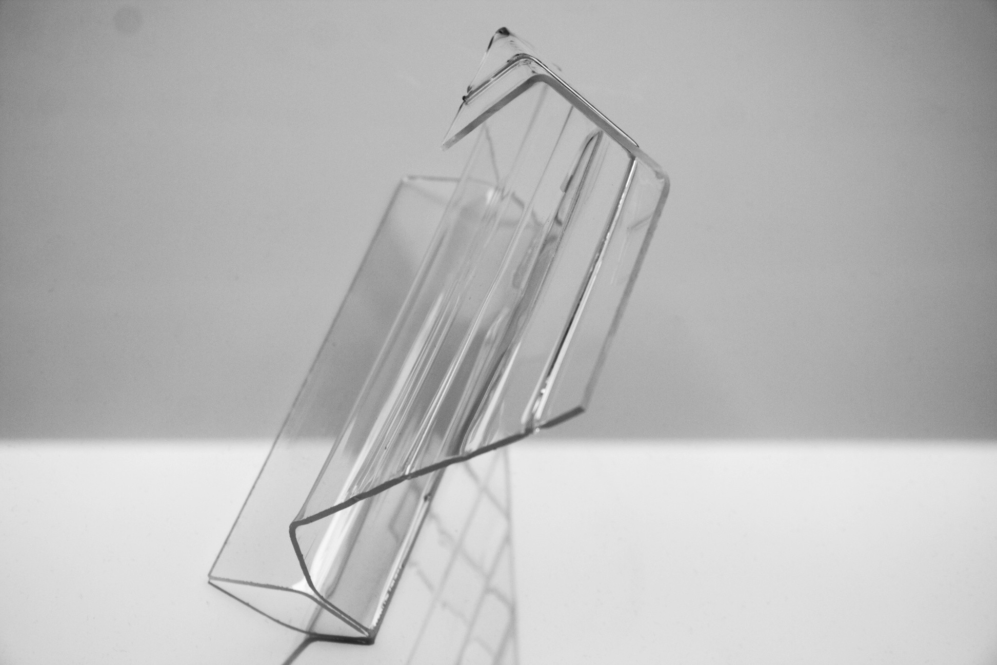 The bending device consists of a 600W IR heater (~45cm in length) occluded with aluminium T profiles and a flat profile wrapped in Al foil and tape in a haphazard attempt to control convective heating of those rails. It works for now but requires cooldown after each bend, so consider a water-cooled solution.
 It has to be determined experimentally how much improvement is needed here in the context of other noise contributions. One can start out with maximum capacitance and investigate individual noise contributions one by one.
 Solid electrolyte tantalum capacitors are more stable in that regard but exhibit higher leakage current.
 This leads to suspect that just hooking up excitation and AVDD to some LDO will in both cases not be enough for proper performance. Capacitors themselves contribute some noise (kTC noise
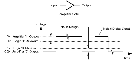
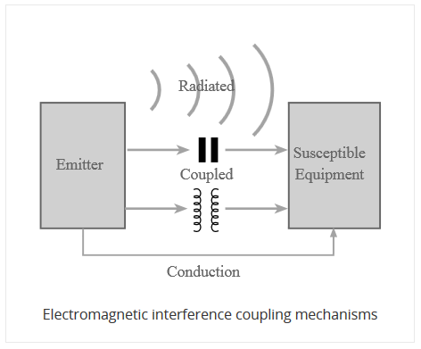
 But I digress. Take-away: open conductor loop areas act as magnetic noise pick-ups while free standing conductors sample the local electric field.
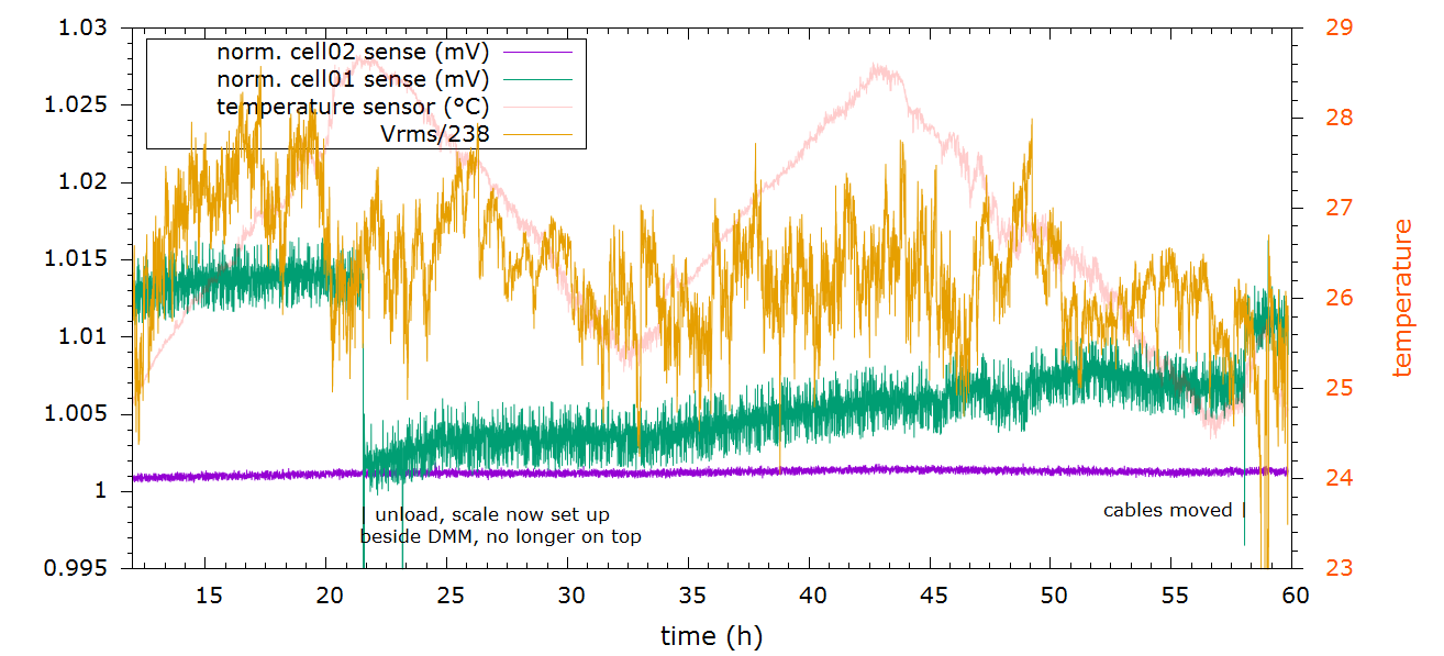
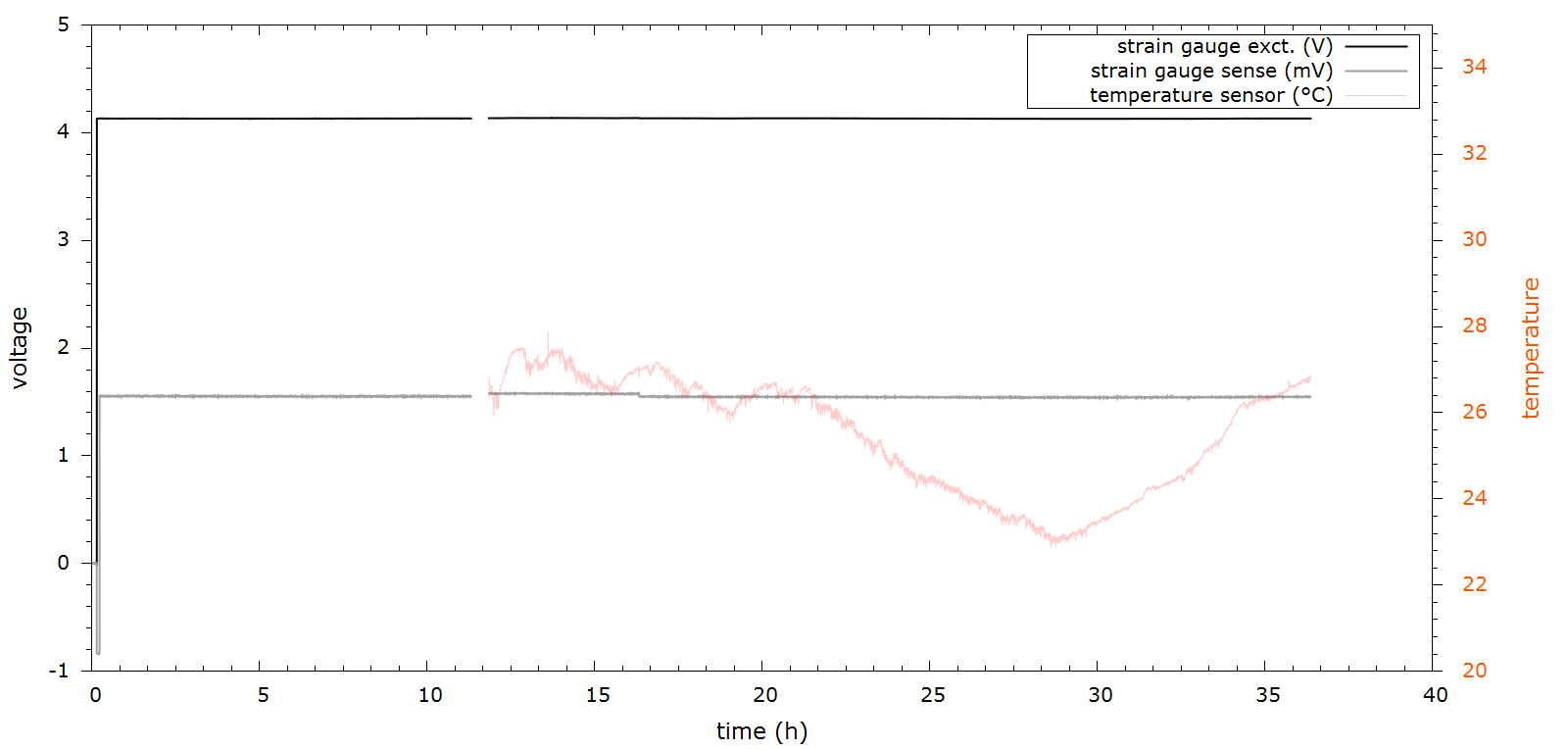
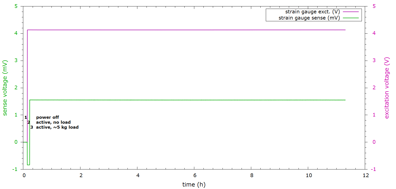
 Once calibrated for excitation voltage drift however...
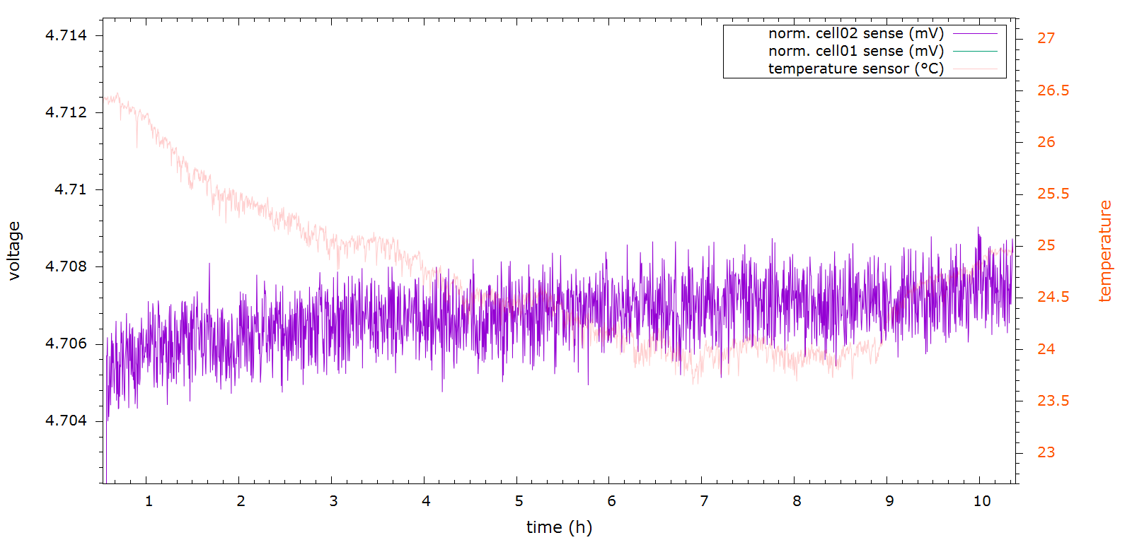 Let's try that again for the 5 kg scale.
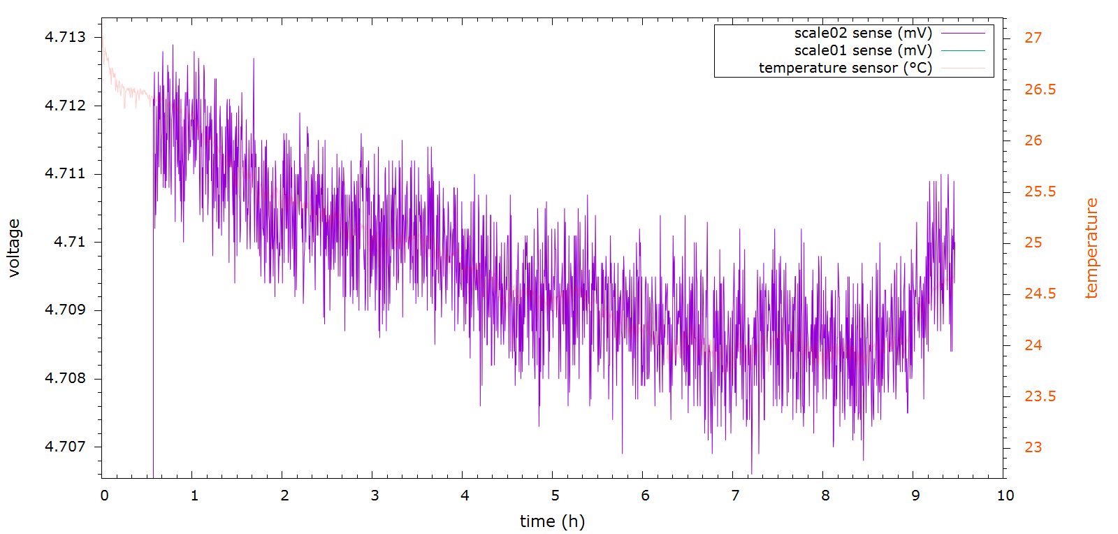
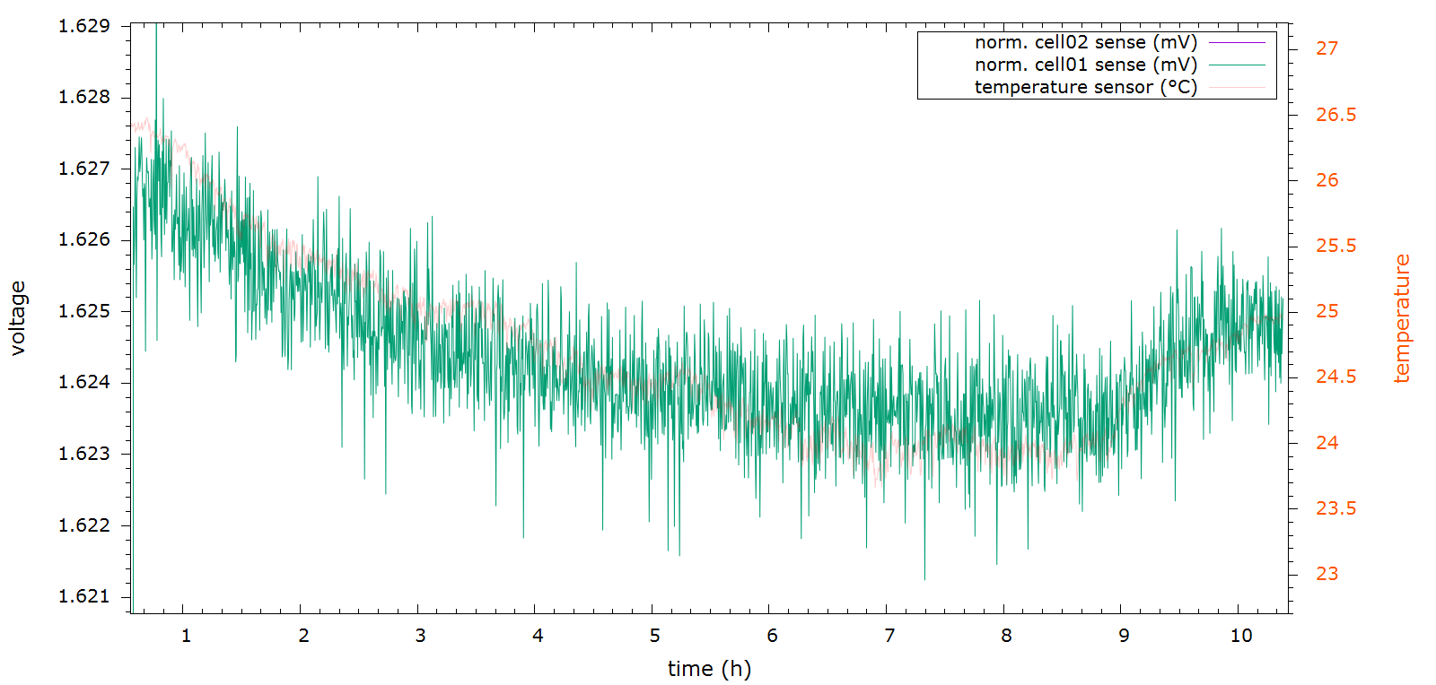 I guess we'll have to have a look at the compensated scale01 sense voltage in the 68h run next...
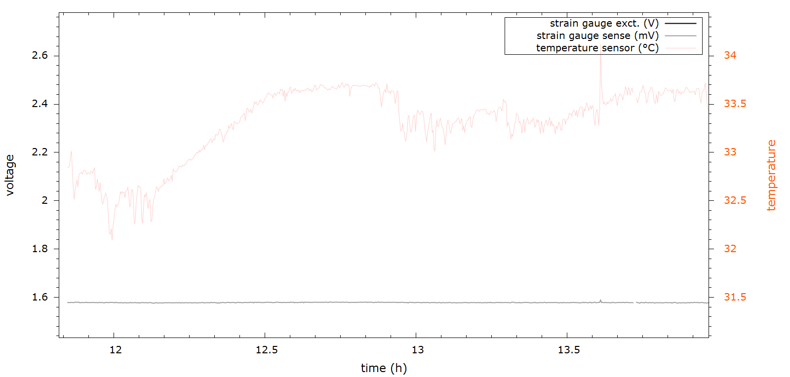
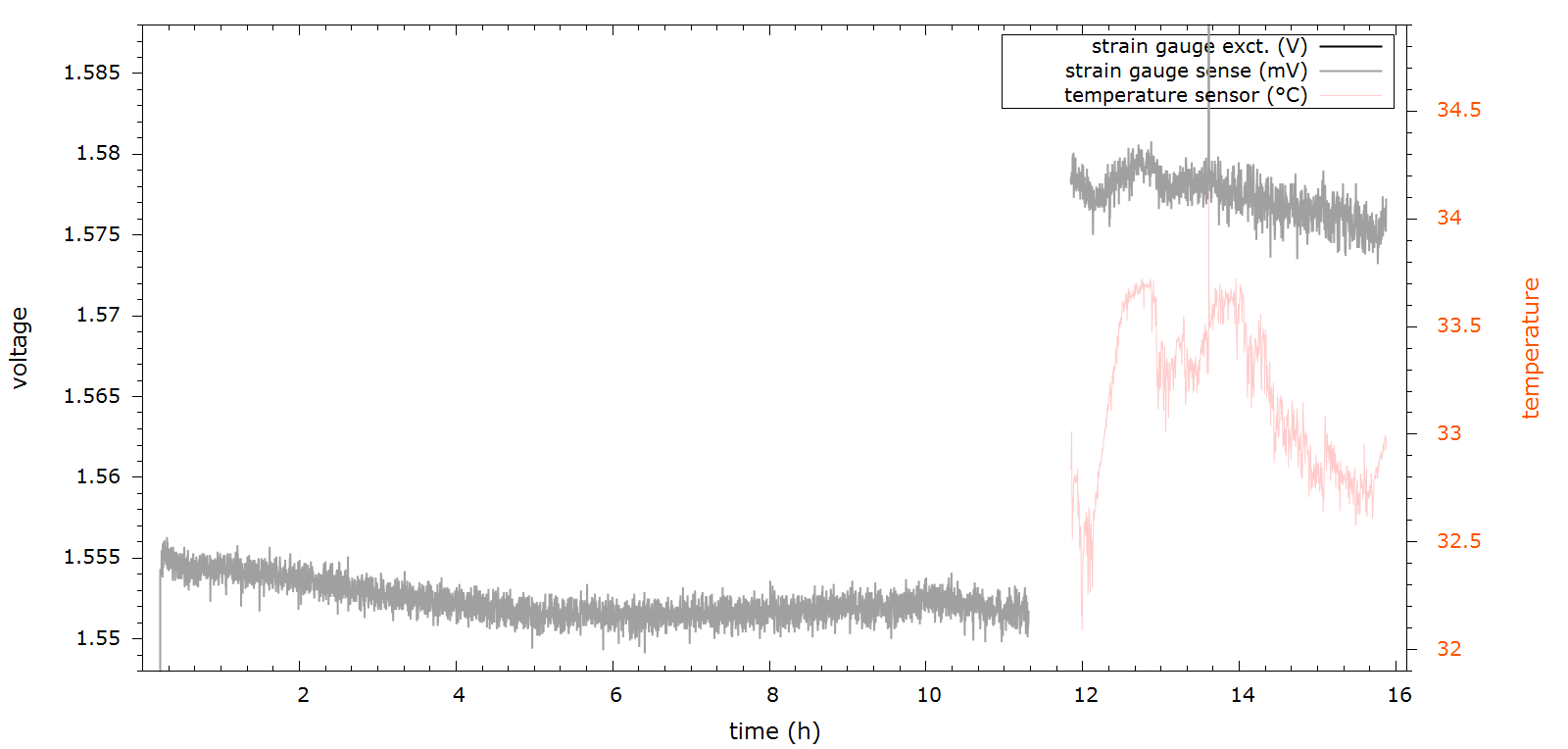
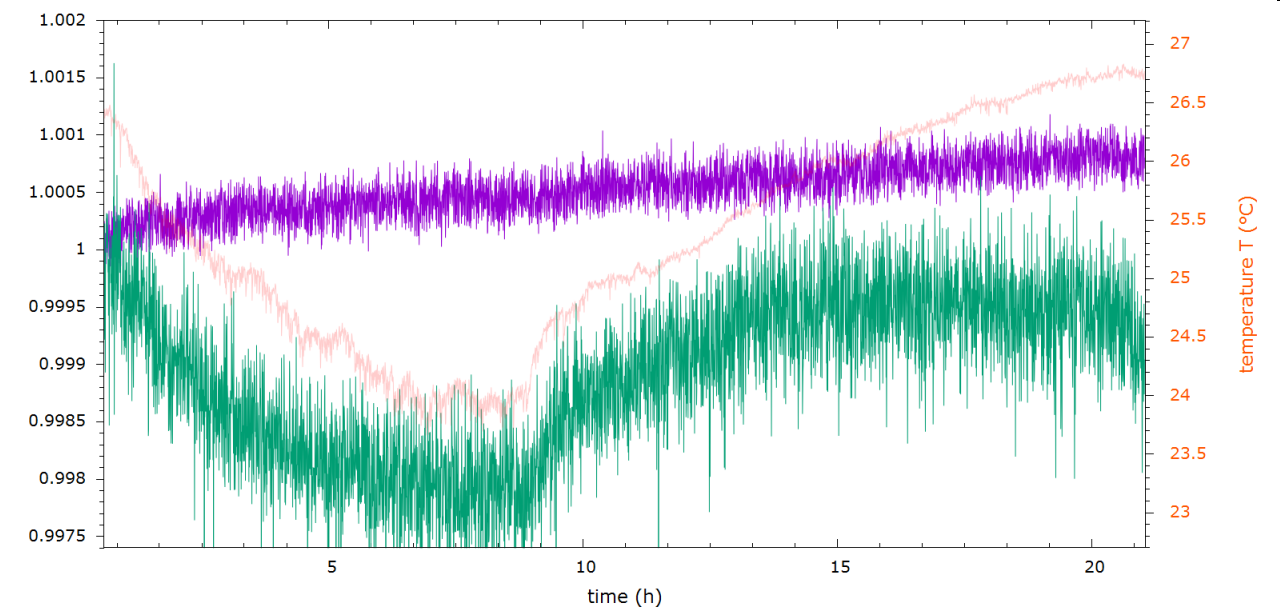 With twice the acquisition time the single point load cell is still just casually walking away from us while the 5 kg kitchen scale is somewhat inspired by daily cycles. I'm not sure whether to call it a temperature effect yet.
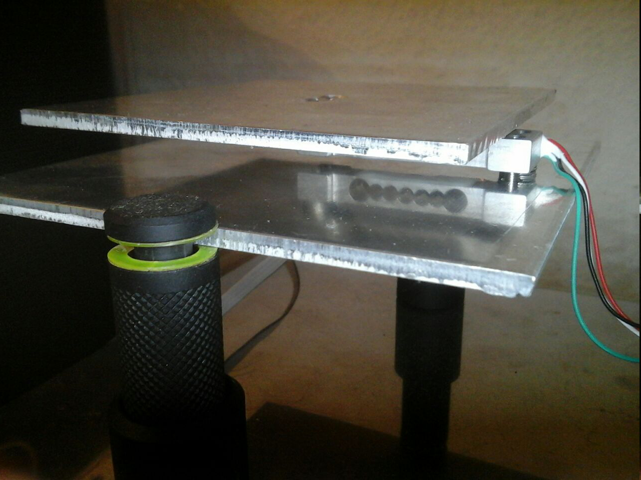
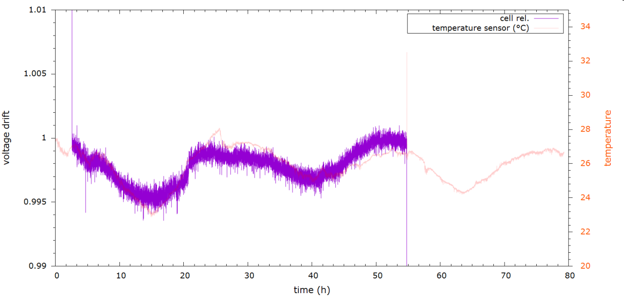 With the kitchen scale having an HX711 board glued onto it vs. the single point scale setup more or less floating in the air, some differences in behaviour are to be expected.
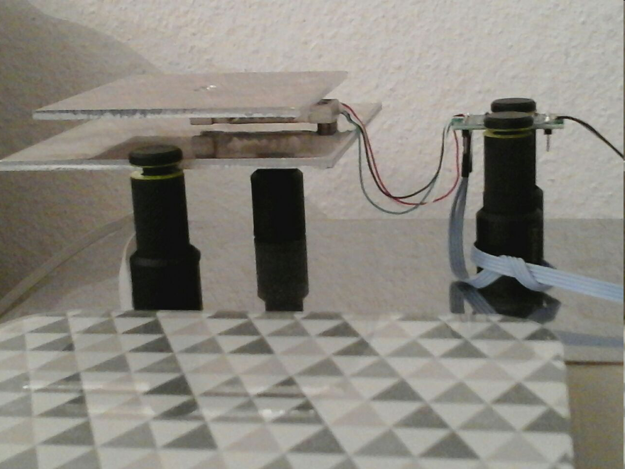
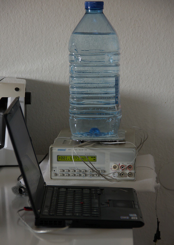
 Just doing a very rough calibration of the mains voltage level it becomes evident that it's not exactly stable even over the course of half an hour:
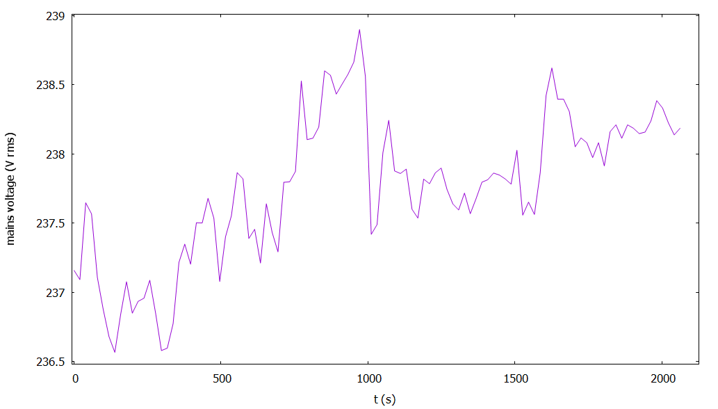 I expect some more drastic day-night variations. What's with the mains voltage? Well.. there's a transformer in the multimeter on which the scale rests, varying in heating power ... I just had to include this data channel. Next I'm pretty sure I'll also have to hook up a hot wire anemometer... driven by an HX711 board... deeper, ever deeper down the rabbit hole :D
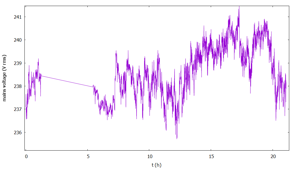
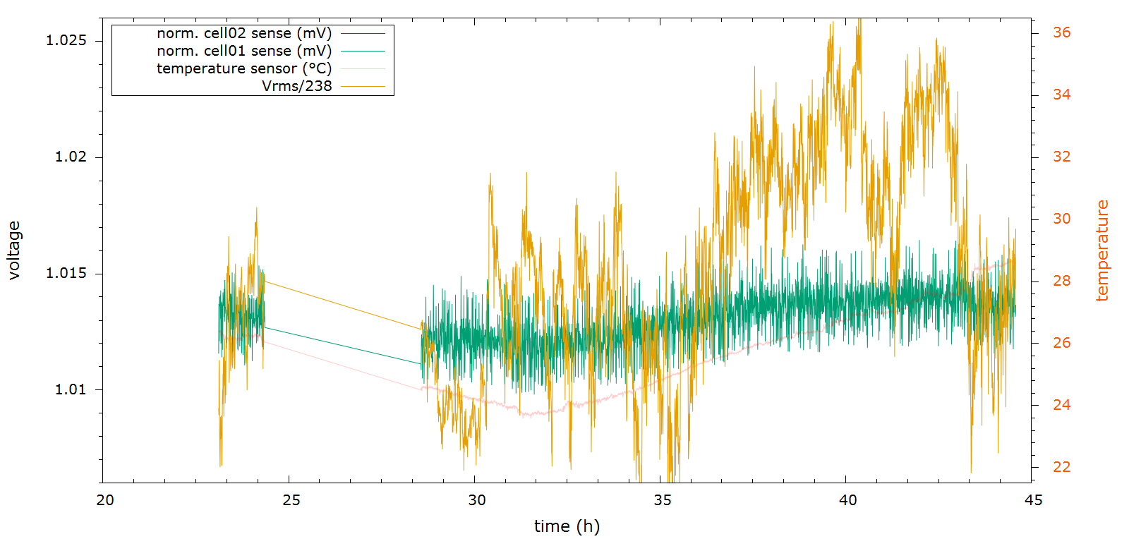 ignoring the wrong starting time for the normalized plot we're not at a point where the far-fetched mains-induced temperature variations are in the graph as well.. and they tell us... nothing? Mains voltage variation induced temperature changes are still minuscule deviations in the mW range.
 Bud Bennett
 insidecircuits