 Owen Trueblood
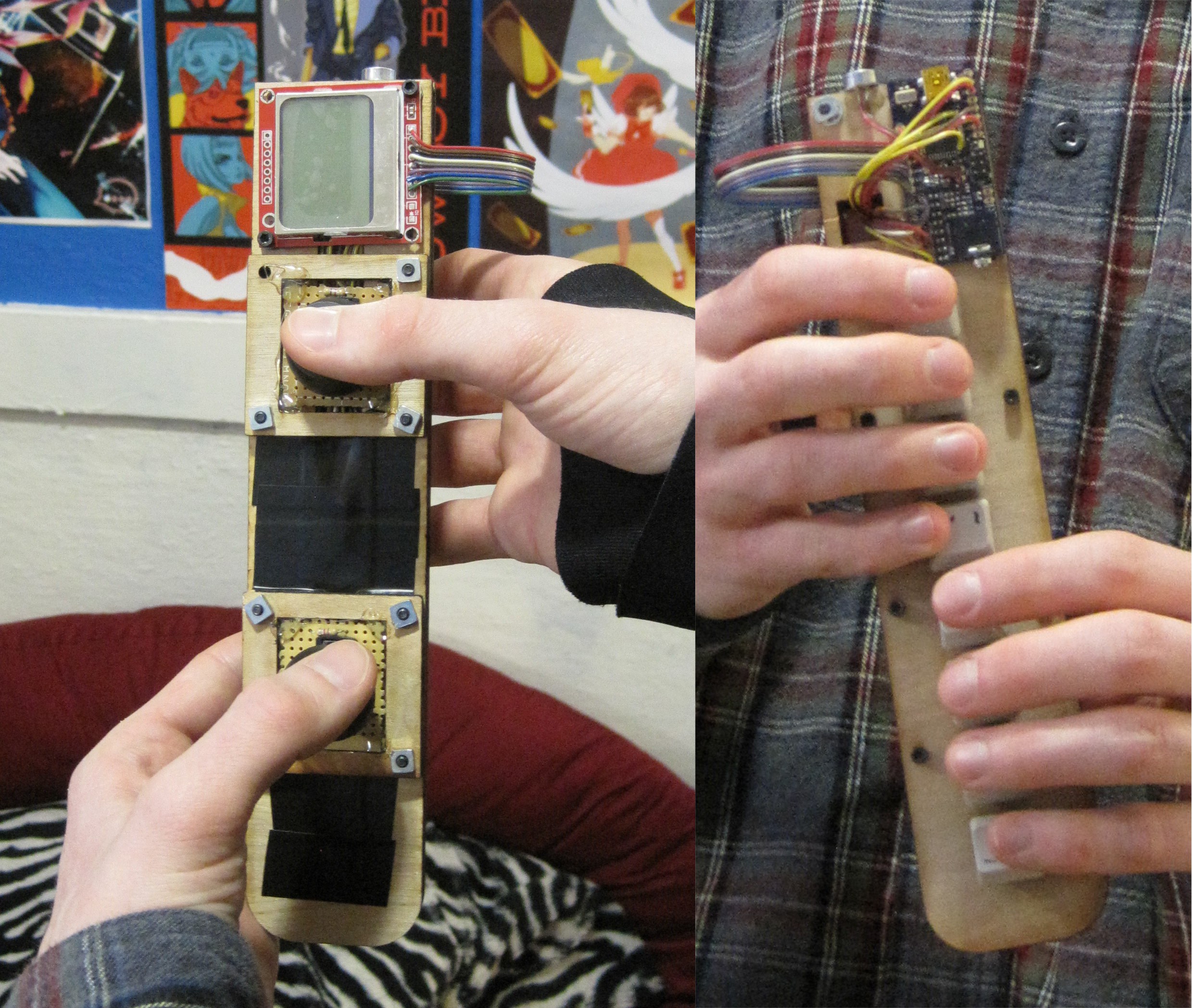
The day before yesterday I finished assembling the electronics and putting them into a laser-cut case.
Mockup
For the first prototype of Grabloop I do not really care about awesome design. I just want it to be comfortable enough to be usable in testing the basic functionality. Later on I will put in the effort to make it look really cool, be really pleasant to hold, and last a long time. So to get started I threw together a cardboard mockup in half an hour or so by tracing the outlines of the various parts and using hot melt glue. I put a little extra effort into making the 8 buttons out of cardboard so that I could position them with tape and find the best layout to match my fingers. I also made the LCD, PCB, and a battery out of cardboard so that I could be sure the real version would have space for those parts.
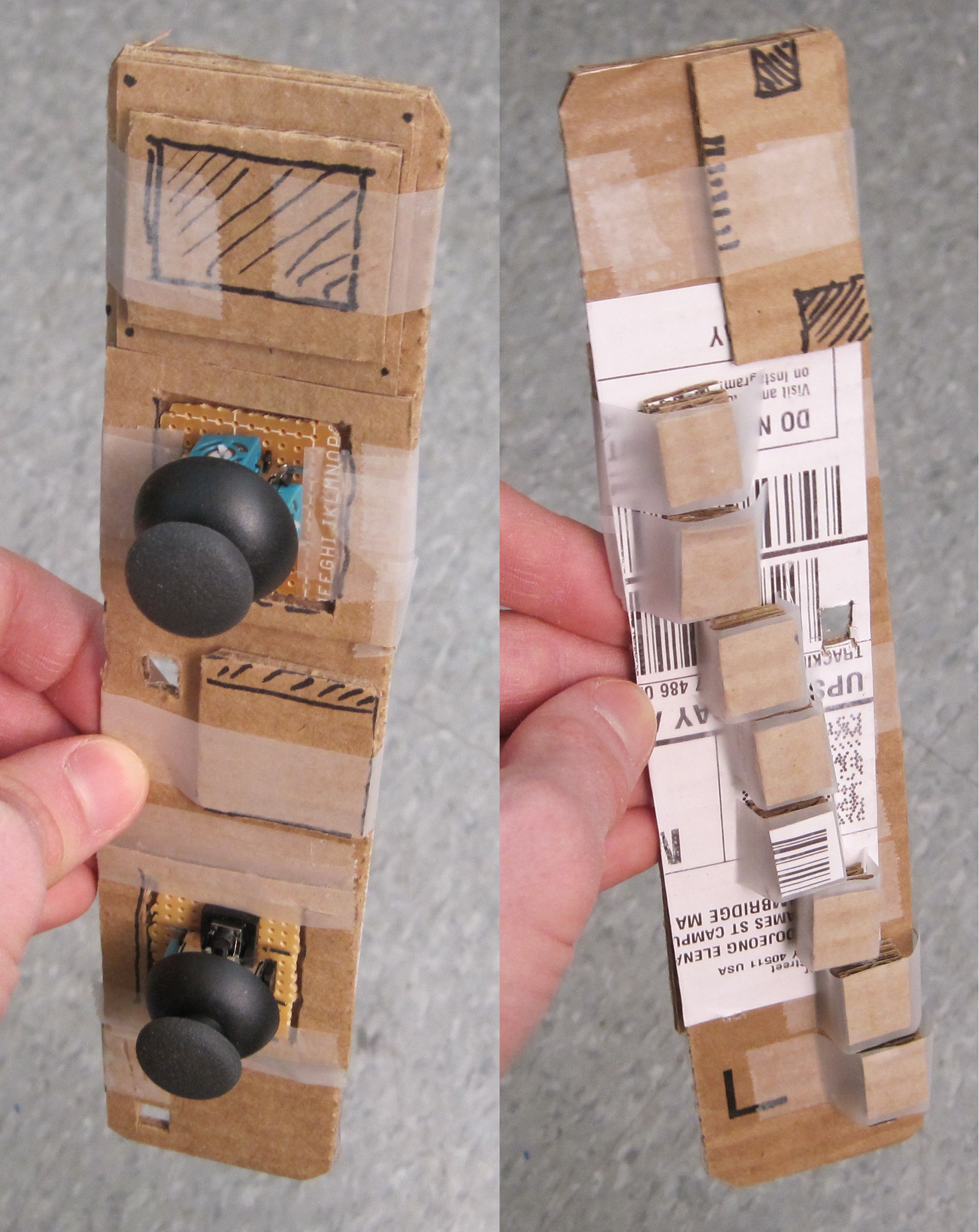
Having a cardboard mockup that can be held is really useful because it makes obvious the little details that matter, like bolt clearance, wire routing, and overall scaling. Any small problem that cropped up could be solved in two minutes with scissors, tape, and glue. When I was CADing the design I constantly referred back to the mockup for measurements, but would round numbers off and shift things around for better symmetry.
Design & Fabrication
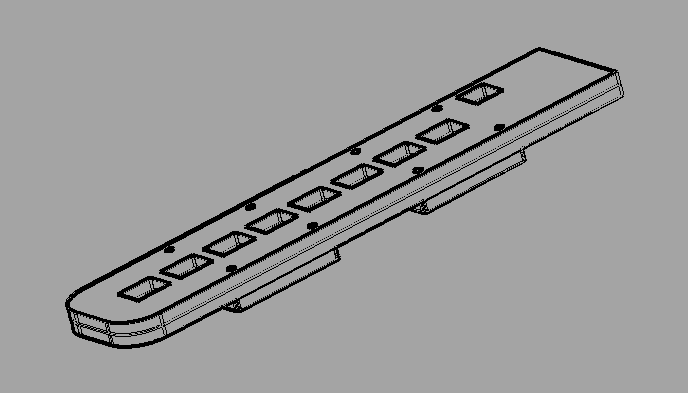
I love making prototypes with pieces of laser cut plywood because it is fast, cheap, and easy. But it restricts the possible design in several important ways. For example, I had to add an extra layer to do the wire routing. And I could not add an extra layer below that one to hide the wiring completely, because it would have made the design too thick. So for this first prototype there are two main layers with a third around the joysticks.
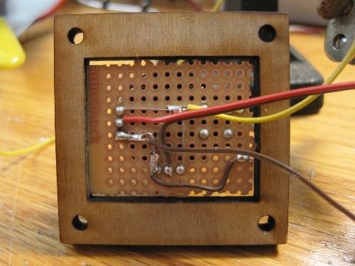
The joysticks were a compromise. I wanted to use PSP-style joysticks to make the grip less wobbly and more compact, but they were out of stock when I was ordering parts. So I used regular stick-y joysticks. The particular ones I got have a button that is pressed when the stick is pushed down, so I soldered a pull-down resistor on the perfboard I used to mount them and routed the two signals to unused pins that I had broken out to test pads on the PCB.
Programming Challenges
Thankfully the AVR showed up the first time I connected my usbtinyISP to the "Audio Rot" board I designed. I used the Arduino software to burn the Leonardo bootloader to the Atmega32U4 for convenience. I am not going to use the Arduino environment to develop the software but their USB bootloader is much faster and more convenient than using the ISP interface. To make USB work properly I had to add a bit of thin lacquered wire on the board to connect UVCC and VCC (I had mistakenly thought they were connected in the AVR) so that the board would get power over USB.
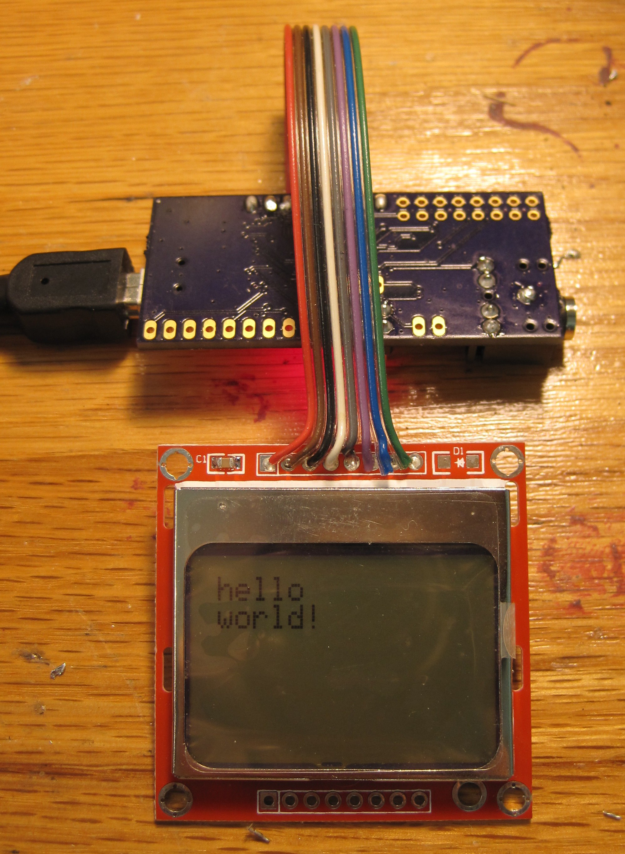
The first thing I tried was driving the Nokia 3310 LCD. A couple of years ago I wrote a nice driver for it in C, so I just copied that and tweaked it for this board. It worked first time, but the contrast was a little off. After a quick dive into the LCD driver's datasheet that was fixed too.
The next thing I tried was generating audio. The board has (had) an MCP4725 DAC connecting via I2C to the AVR. It took a couple of hours of debugging to make it work because I could not figure out what the static customer address bits were, and more importantly I neglected to put pullup resistors on the I2C lines. I think my reasoning was that with one master and one slave it would just be a matter of the master serving the same purpose as the pullups and keeping the lines high during idle times. Maybe that would have worked if I wrote my own I2C driver, but I did not want to bother with that so the pullups were necessary.
But once I had the DAC generating a signal I ran into a much worse problem. The chip summary had stated >3MHz data rates, so I had thought to myself, "well, I only need 48KHz for audio so that should work fine." But in practice I could only generate a tone as high as 3.5 KHz. Why? Because it takes a lot of bits to push a sample to the DAC. Start bit, 8 address bits, 16 data bits, ack bits, and a stop bit. So that already divides the rate by about 30 (to 6.67 KHz). On top of that, the >3MHz rate is referring to the high speed mode of the I2C spec, which must be activated and reactivated on every transmission with a special extra byte. So there was no way to generate the nice audio I wanted. As a fix I desoldered the DAC and soldered a wire from SCL to the output pin, taking advantage of the fact that SCL is also OC0B (PWM) on the Atmega32U4. The audio goes through a low-pass filter, so even as just PWM it has the chance of sounding okay.
With tones coming out of the jack on the board I set about making the microphone work so that I could do a pass-through of audio and hear something more interesting. This is where I ran into my latest lazy-pcb-design problem: the amplifier circuit does not work properly at all. I saw the unamplified signal coming from the electret microphone pass through the low pass filter on the input. I followed it all the way to the op-amp. But the output of the op amp was a very steady 2.5 volts. No amount of yelling into the mic could get it to wiggle at all. So I took a good look at the circuit I had copied from a Sparkfun breakout board. My analog electronics skills are still in their infancy, but to me the circuit looks like a buffer that will maintain the 2.5 volts given to it by the voltage divider on its positive input. Obviously something more is there because Sparkfun's breakout board does work. I think that that something is the FET and variable capacitor making up the electret mic, but I do not understand how the mic changes the amplifier circuit.
After doing some simulations that showed no amplification from the Sparkfun circuit I was still mystified, so I looked for circuits that worked for other people. Seems like standard inverting amplifier set-ups work fine. So my plan is to breadboard an inverting amp, check it works with the mic, and then rearrange parts on the PCB to implement it. If I spend a bit of time I am pretty sure I can find a redesign that will minimize required solder-fu.
Lots of lessons learned from working on this PCB (one of my first ever). I am getting a sense of what level of laziness is acceptable and how difficult it is to repair mistakes that crop up in PCB design. For this board I just spent a few hours throwing the PCB together, making up the circuitry as I went along, so mistakes like the ones I ran into are acceptable and even useful (for learning). But in more serious future PCBs I now know about some more issues to look out for.
Discussions
Become a Hackaday.io Member
Create an account to leave a comment. Already have an account? Log In.