The new revision PCBs and new inductors came in late last week.
For comparison sake, I replaced the 100uH inductor with a 33uH inductor on the rev 1 PCB. The AL8861 data sheet lists 100uH as a legal inductor value, and I wanted to keep the operating frequency as low as possible, to keep spurious RF emissions down, so I started the project using the 100uH inductors. The example schematic diagram in the data sheet and both revisions of their eval boards used 33uH inductors. Anyway, the rev 1 PCB with the 33uH inductors worked better. There was less noise on the switch node waveform, and the current controlled better. There was still enough noise on the switch node to cause problems at high current though.
The rev 2 PCB has several improvements over the rev 1 board:
4x the capacitance on the input power supply.
Got rid of the Schottky diode in series with the input power.
Lots more copper on the power distribution network.
Lots more copper on the switch node (U1 to inductor L1) connection.
Footprints for capacitors across the LEDs and the current sense Resistor.
Tighter layout of the current feedback net.
After building up the the rev 2 board with the 33uH inductor, it works much better. The input current shows almost no AC on it at all - the additional input caps solved that issue. The noise on the switch node with 1 or 2 LEDs is gone, it is a variable duty cycle square wave. The current to the LEDs, even with the long wiring in the goosenecks is very clean. Curiously, it looks more sinusoidal than triangular. This may be a consequence of the capacitor that I put across the LED connections on the new PCB forming a resonant circuit.
For comparison, here is the old schematic:
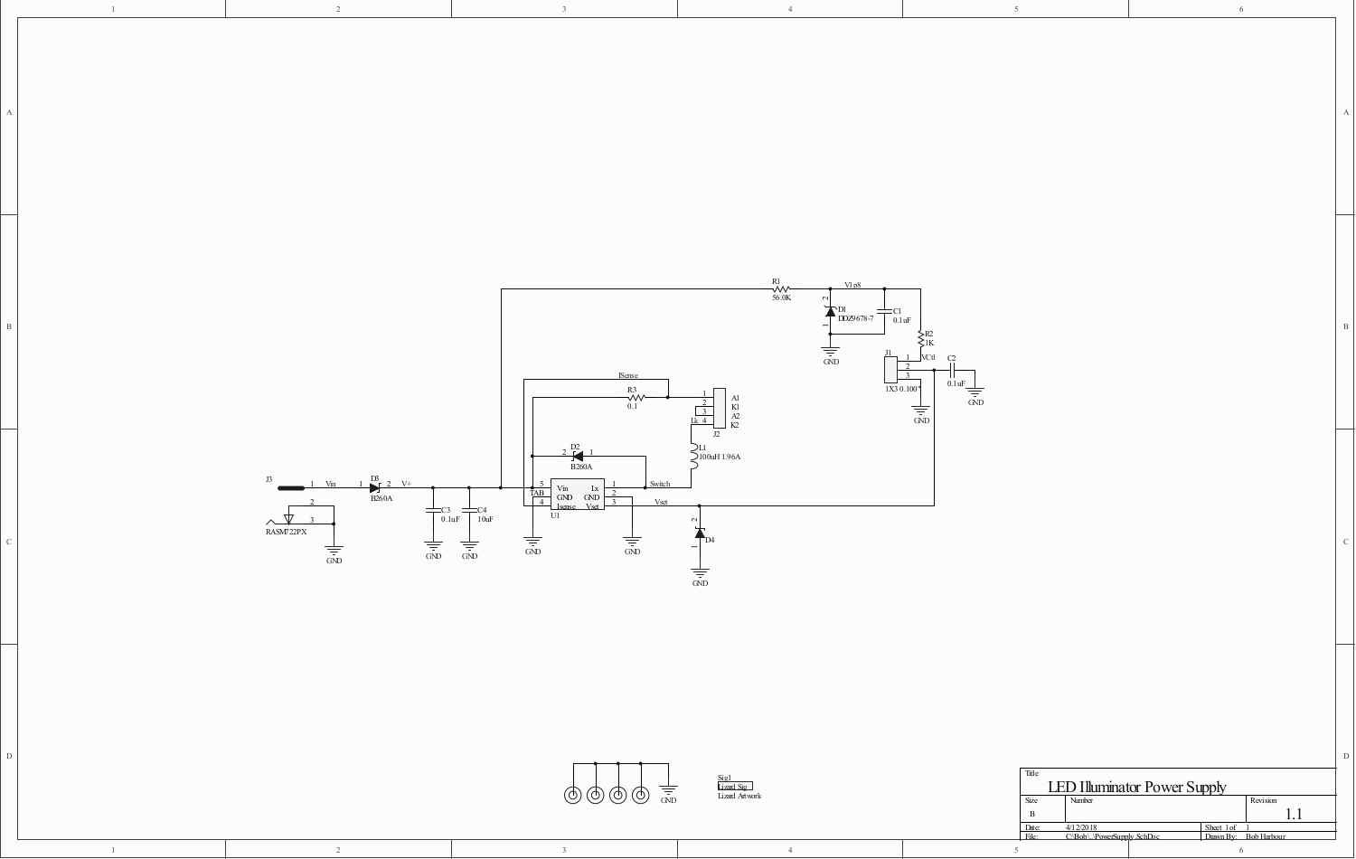
Next, the new schematic with the additional input capacitance and the caps across the LED connector and the current sense resistor. The cap across the current sense resistor was not placed when the board was built and does not appear to be needed.
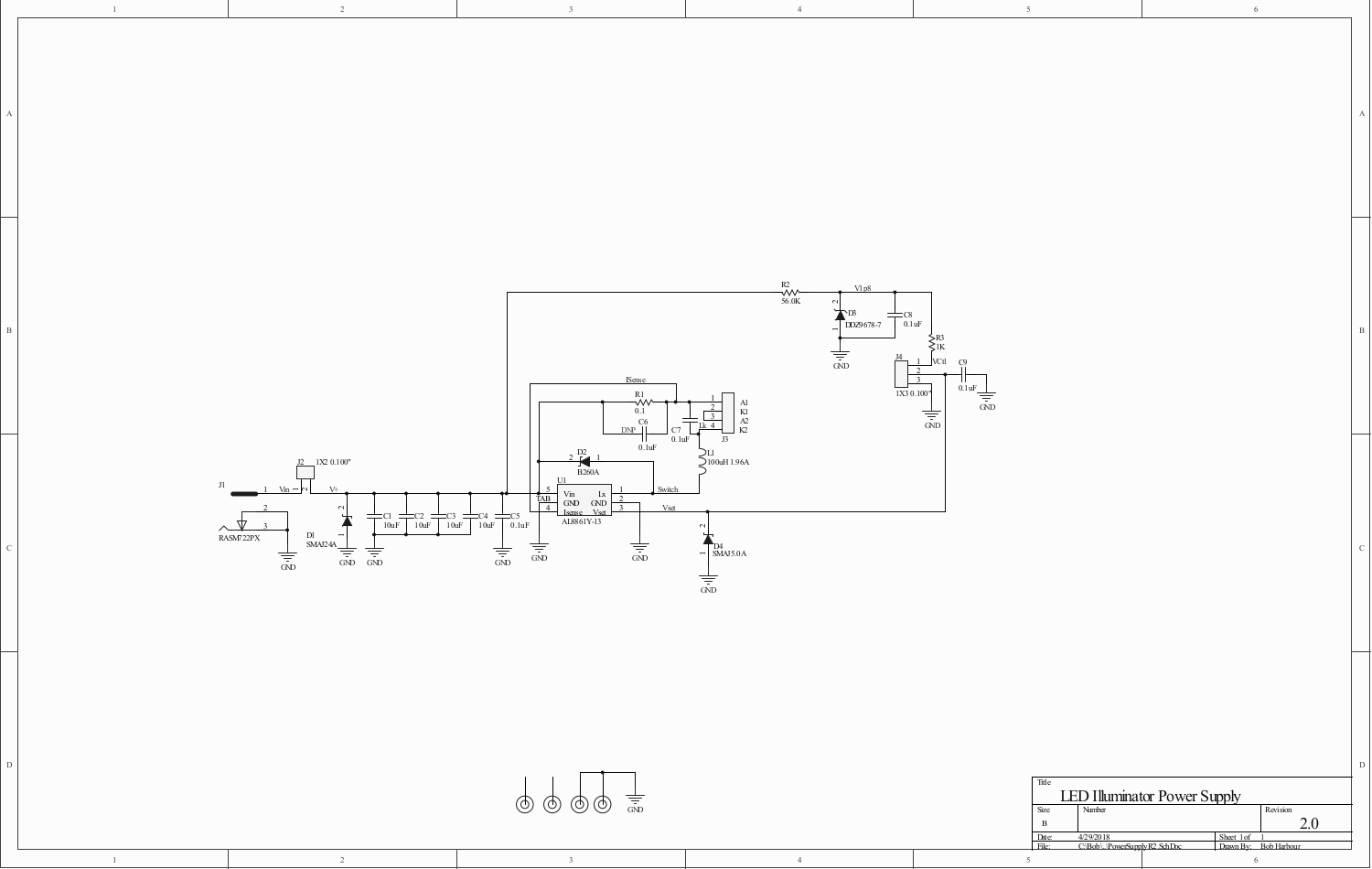
The inductor L1 on the second rev board was populated with a 33uH part instead of the 100uH part. Also, resistor R3 was populated with 4.4K rather than 1.0K to reduce the maximum current setpoint.
Here is the rev 1 PCB layout. The power distribution between the input connector J3 and D3 anode is only 0.050" wide copper on the top (green) side of the board. Similarly, from D3 cathode to R3, D2 cathode, C4 and U1 pin 5 are 0.050" wide or less. The current sense trace is the skinny trace between R3 and the Lizard can be seen looping around a fair area.
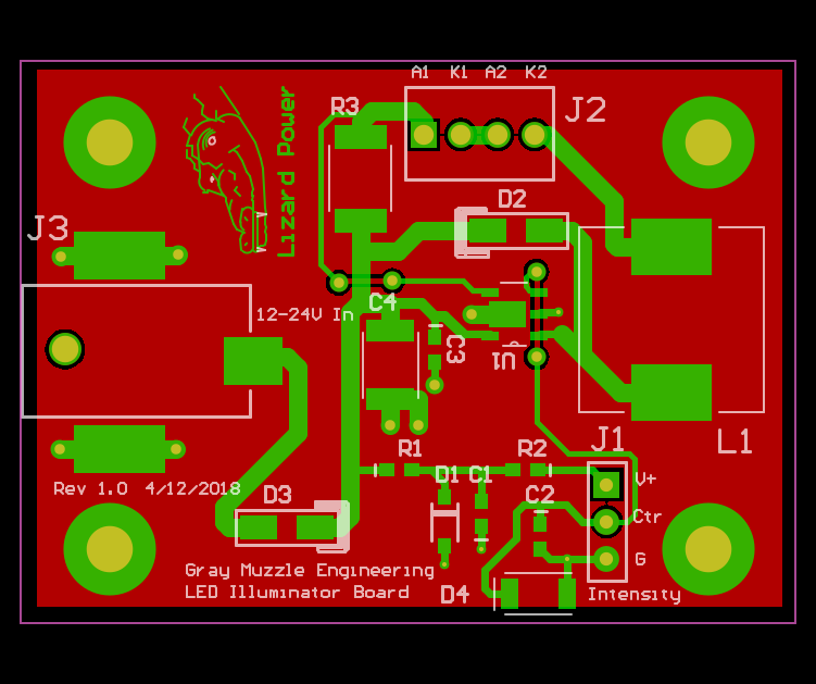
Below, the Rev 2 PCB layout can be seen.

The 0.050" power distribution was replaced with polygons, offering lower impedance between the 4 input filter capacitors and the rest of the circuit. The current sense trace runs mostly on the bottom side of the board (red) and has less loop area, providing less opportunity for noise. Both the U1 to L1 connection and the L1 to LED connector are heavy polygons for lower impedance.
Between the new PCB layout and the lower inductor value, the performance of this power supply is acceptable now. Scope shots of the switch node voltage (ch1) and the inductor current (ch2) look pretty reasonable. The scope shot below is running at about 135mA of LED current. The previous board would operate at this level.
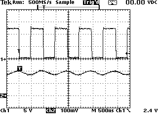
The next scope shot shows the power supply running at about 375mA of LED current.
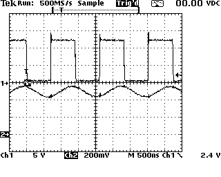
With this much LED current, the previous board would be showing an unacceptable amount of noise and getting hotter than I like. There is still a small amount of ringing on the switch node voltage when the switch turns off and the current begins flowing through D2, but this is not unusual in circuits of this type, and I am going to live with it. The new board runs cool, barely above ambient temperature. Sadly there was not enough room on the top side of the board for the Lizard...
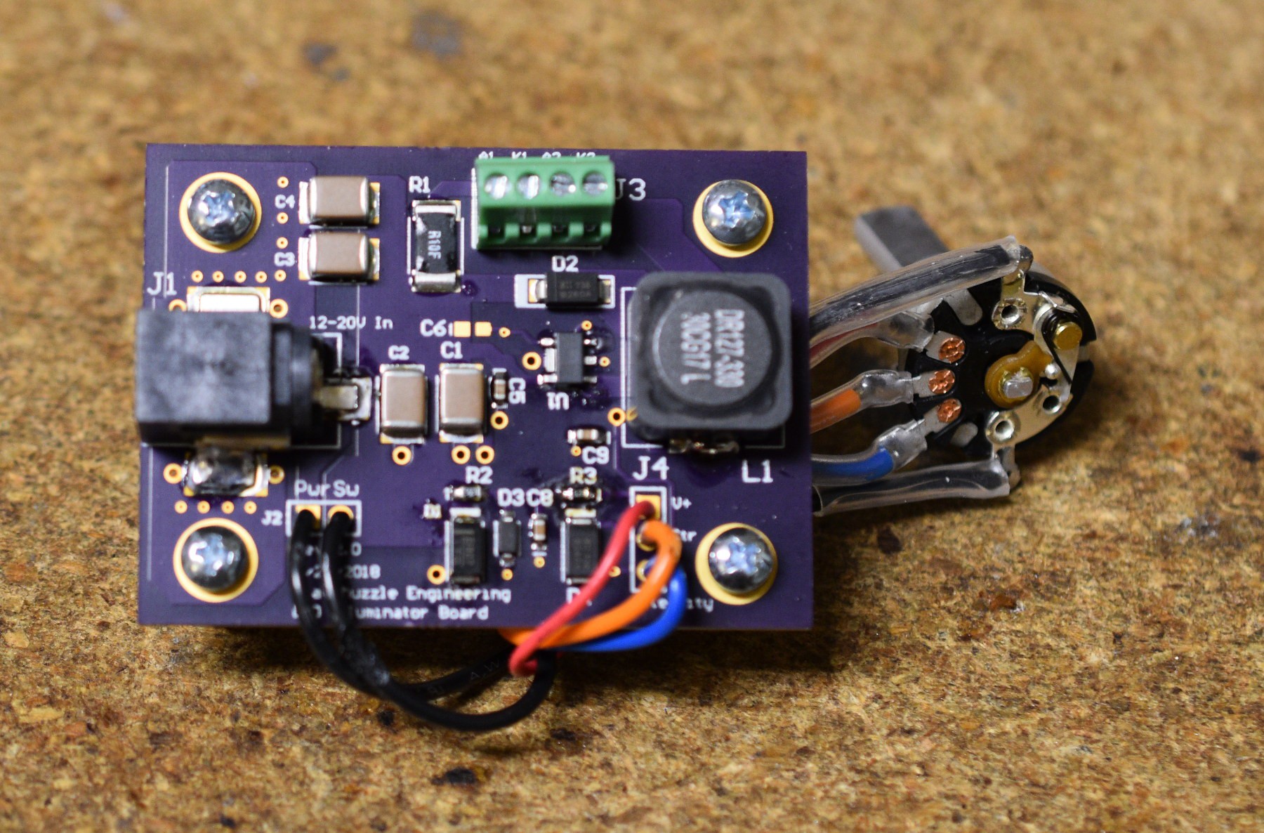
During testing, one issue showed up. One side of the LED wiring is connected to the positive power rail. The chassis and goosenecks for the LEDs are connected to the negative power rail. There is not a lot of clearance around the LED mount PCBs, and one of them shorted the positive wire to the chassis. This happened while it was powered from a current limited lab power supply, so no damage was done. To prevent problems in the future, I added a 1 Amp fast blow fuse to the positive wire going to the LEDs.
The next step is to build an enclosure to house the power supply and mount the 2 goosenecks with the LEDs on them.
 Bharbour
Discussions
Become a Hackaday.io Member
Create an account to leave a comment. Already have an account? Log In.