 Ben Jordan
We easily assume based on public comment that in general, hardware designers hate (or at least ignore) autorouters.
But scratching into the surface of normal conversations with intelligent, pragmatic hardware engineers and inventors, reveals a common opinion that we would expect in 2018 that autorouting could actually be useful. Problem is, some EDA vendors haven't really done enough to teach users how...
Well, even with somewhat outdated technology, if you know how to set it up you can actually get acceptable, even good, results.
Autorouters are useful not just as an all or nothing proposition either. They can be a tool for the following:
* Iteratively check how good is your component placement and orientations.
* See for a given density and available layers, how hard is this board going to be to route.
* Figure out how many layers you might need.
* Fanout and escape routing)
* etc.
This is a big subject and to be honest, I'm doing this at the request of Sophi Kravitz, and at this beginning stage it feels like I'm about to try and boil the ocean.
Having said that, I am doing this because it needs to be done. I sincerely believe people will benefit from knowledge gained and captured in this project, and I want to encourage others who have experience with vairous automation to contribute. This is not about promoting Altium tools, it's about promoting the acceptance of routing automation and helping everyone get more efficient use out of technology.
PART 1 - RULES abd CONSTRAINTS
The autorouter has to follow design rules and constraints. Obvisouly therefore step one is to configure the design rules. I'm providing here the bare minimum. However usually the bare minimum is all you want - if you over-constrain the design the autorouter will spend a lot of time to give you not much of a result. It's contentions will be higher and completion lower.
Bare in mind - if you can't manually route the design, no automation will be able to either.
Most EDA tools begin a new PCB layout with a set of reasonably conservative rules/constraints by default. This is the case with the tool I'm using for this project (CircuitMaker by Altium). Therefore I am making the assumption you too have a standard set of default rules which is reasonable. So I'm not going to explicitly go over every rule in detail. I'm just going to cover the specific few rules which I use or modify for working with the Situs autorouter in CircuitMaker / Altium Designer. Your mileage may vary.
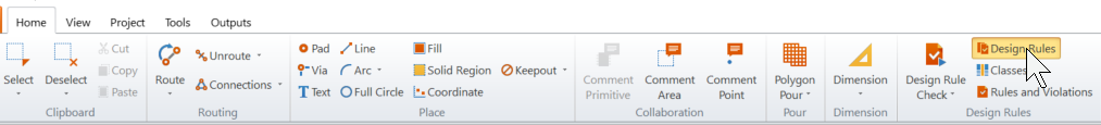
For those who are "following along" in CircuitMaker, I'm opening a PCB and clicking in the "Design Rules" on the Home ribbon:
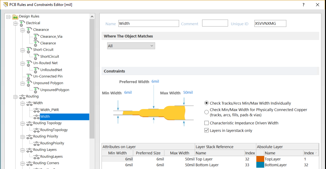
Clearance
Set up the clearance rules. Autorouters can and will do unexpected things with vias and traces if you don't do this. Electrical clearance at a bare minimum will space things according to an object-to-object table. My defaults are for 10 mils spacing which is way too broad for some of the chips I'm using like the USB UART bridge in this design. Therefore I set all objects to have a default clearance of 6mils (still reasonably conservative for any fab with oil in their lamp). Then I set broader clearance (10 mils) where there will be pads and vias - I don't want those too close together:
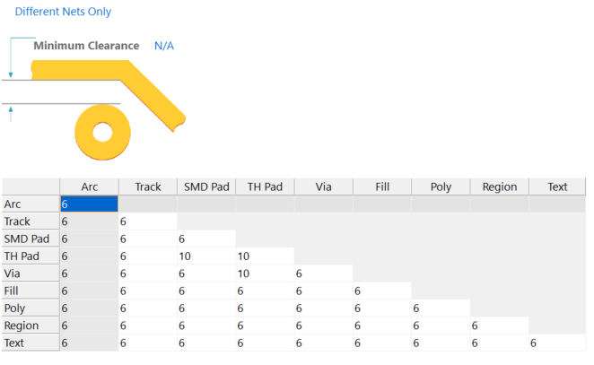
KEEPOUT
Note that the clearance rule is also applied to "Keepout" objects. Every EDA tool I've messed with has this kind of notion - there are rattle snakes and you must stay away from them! So, for the prupose of a proper demo I am adding a keepout to the basic PCB outline so that routing won't cross the board edge boundary:

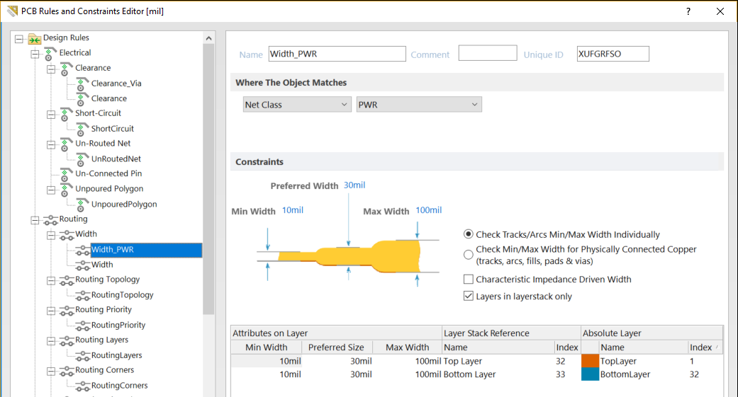
Track / Route Width
I also need to use reasonable track widths. The default rule for trace widths is also 10 mil, which is rediculous for power supply nets. (See my other blogs on setting trace width - calculating widths is outside the scope of this project).
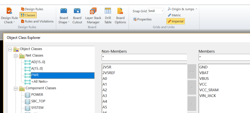
I have seen many designs where the designer had several complex rules for trace width. In most designs this is unnecessary complexity. Unless you're doing a section of DDR or something high speed, you can keep things fairly simple according more to manufacturability. For the few high speed signals you can also limit your rules and scope those. For now, let's just use a simple rule for general routing and another scoped to the power supply nets which I have grouped into a net class called "PWR":
Via Definition
In many EDA packages the size and shape of pads and vias is driven by "pad stacks" or other library notions. But in Altium tools like AD and CircuitMaker it's more programmatically defined by the Design Rules. As with clearance and width you can scope different via styles to different net classes, so if you wanted larger vias for power nets you can easily setup multiple rules for that.
My personal preference however is to keep it simple with a single, small via style across the entire design, and in the cases where I need more current handling to cluster more vias for power and ground. For the purposes of learning autorouting I'm just using the one rule:
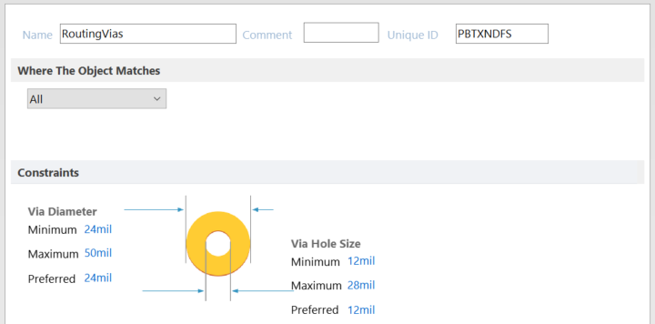
This rule means I am allowed to place any via manually in the design between 24mil and 50 mil diameter, with holes ranging from 12 mil to 28mil. When we run the autorouter it will choose the "Preferred" parameters, so I am electing those to match the minimums of 24mil via with 12mil hole. This is still fairly conservative - any decent fab including OSH Park or PCB Cart will have no qualms with this via size.
Others to Play With Later
There are several other rules which are used to direct the Situs autorouter, however for now I will keep them at their default settings and just name them here. We will come back later and explore some of those when we go beyond 2 layer boards, as that's when they'll be more needed.
They are:
- Routing Topology: Defines the connectivity graph's physical orientation for the scoped net or net class (or all nets by default). This can be used to bias the routing connection styles between shortest path, daisy-chain, daisy (mid driven), Horizontal, Vertical etc.
- Routing Priority: Can be used to control the order of routing for different nets or net classes. For example you can give higher priority to a specific bus than other low speed or less important nets, or power supplies, etc.
- Routing Layers: This rule can simply enable or disable different layers and can be scoped to different nets or classes as well. So this will be useful later on when we want to separate power and ground routing to internal layers on a multilayer PCB, for example, and for high-speed nets like Ethernet and USB when you want to keep them entirely on the outtermost surface layers of the board for signal integrity reasons.
- Fanout Control: Fanout means building short traces out from component pads and then placing a via, so that big hairy components like BGAs can have a nice set of "dog bones" which breakout the signals to other layers on the PCB. Many designers won't autoroute the whole board but almost everybody will use the Fanout pass at least, because it will help you route those BGAs (and other find pitch components) much easier.
IMPORTANT: Rule Priorities
I'll finish out this "step" with one final note about design rule priorities. In a rules and constraints system like this, it's highly flexible and configurable, and as such you can have multiple rules and you might end up with different rules and some not being properly applied. This is because when you have more than one rule they are processed first in order of "priority" and then within each rule only the objects that are scoped will be processed. If you don't pay attention to this, it means you may have ineffectual rules, or worse, some objects in your design that never have rules applied.
Here by way of example is the default set of "Fanout" rules. With the selection on the rule category "Fanout Control" (to the left) you see the list of rules defined for that category. Priority 1 means that rule is processed first in the sequence. If then, the priority 1 rule had a scope of "All" it would have the effect of all the other rules being ignored, because all the design objects would be applied to the first rule, and the rules engine (and router) would not process the list any further.
This also means that the last rule is a catch for all the other objects in the design (in this case, all the other types of footprint). Some rules should always have an "All" scoped rule at the end: Width, Clearance, Unrouted Net, Routing Vias, Fanout, etc. because if they don't there will be some design objects which have no important such rule applied and the system, and you the designer, will not know what to do with them.
That's it for now, for step one. I will now demonstrate with the results of this step, what actuall happens with autorouting two memory devices and a latch from my example design.
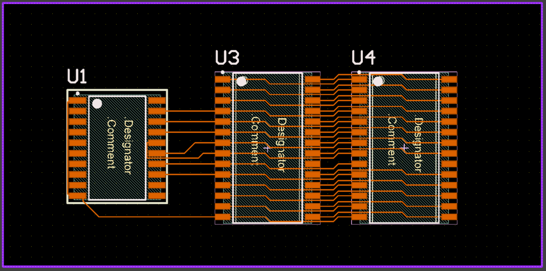
We will come back to this but for now, this is the "Memory" routing algorithm which looks for lots of parallel connected lines and does them spaced evenly. In this example no vias or layer changes are necessary!