One-Off Solder Mask
This document outlines how to take an EAGLE layout, a printed circuit board manufactured using the Protomat C60 circuit board cutter, Kapton tape (1 mil thick), and a Universal Laser VLS 3.50 to create a solder mask for your circuit board. Figure 1 shows the finished product; a cut circuit board covered by amber-colored Kapton tape forming a solder mask.
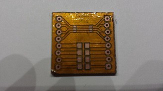
Figure 1: A circuit board fabricated using the ProtoMat C60 PCB cutter with a Kapton tape solder mask attached, leaving only the pads, vias, and lands exposed.
The work-flow to accomplish uses the following software packages, in order, EAGLE CAD, Corel Draw, and a Universal Laser VLS 3.50. This document is structured along the work flow from start to finish.
Eagle
In order to test the Kapton tape concept, I used EAGLE CAD 6.4 to construct the circuit in Figure 2.
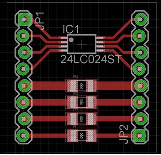
Figure 2: The circuit board used to test the Kapton tape solder mask concept consists of a TSSOP part, four resistors in a 1206 package, broken out onto headers.
The header pins rows are separated by 0.7” making them easy to install in a breadboard. The outline of the board is a square 0.9” on a side. I chose a combination of thru-hole and SMT components because the footprints are fundamentally different. SMT devices have both a tCream and tStop layer, while thru-hole components only have a tStop. This difference results in some extra steps in the following work flow. Finally, I selected the TSSOP packaged EEPROM because it’s the tightest pin pitch (0.65mm pitch with 0.23mm pin width) you can produce on the ProtoMat C60 PCB cutter. The resistors R1-R4 are standard 1206 packages.
Note I will refer to copper to which SMT devices are soldered as lands. The Kapton tape must be open over the lands and solder paste deposited in these areas. There are exactly 16 lands in Figure 1; the round holes for the thru-hole are not called lands, in part, because we will not be putting solder pates on them.
This is not a tutorial on creating a schematic and layout in EAGLE; it’s assumed that you have a completed layout like that shown in Figure 2. Once the layout is complete, you will be working with two tools in EAGLE, the Design Rule Checker (DRC) and the CAM post processor. We start with the DRC.
In order to create a solder mask for a board containing both SMT and thru-hole components, you must work with the tStop layer DRC and possibly the tCream layer. Let’s look at the simpler of the two first, the tStop layer.
In the lexicon of EAGLE CAD, the stop mask is what we are calling the solder mask. EAGLE CAD gives you the ability to make the stop mask larger using the Masks tab in Tools->DRC… as shown in Figure 3. Note that the figure shown on the left side (in this case a SMT pad and thru hole) depends on what cell is active. Unless there is some other need, set the Stop mask to be 0mil then the land or pad it’s over.
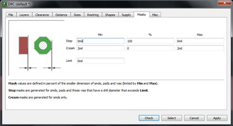
Figure 3: The stop mask settings for your design should set both Min and Max to 0mil.
Note, the longpads version of a header in the sparkfun library generates invalid output by the postprocessor (when exported as an encapsulated postscript file). This may not be an anomaly with this part, so make sure to verify that you have a valid solder mask before cutting your PCB. In my case, I was able to switch to a circular footprint and everything worked fine.
The following discussion on the tCream layer is only necessary if pullback for your SMT components is needed. If you don’t know what pullback is, then keep reading. During the cutting process, heat from the laser will eat into the borders of the cut making them larger then what you wanted. I will call this excess width kerf. Kerf is a problem because, with fine pitch components, the kerf from adjacent lands may eat away all the solder mask between the pins, causing the two lands will join together into one big open area. We can partially compensate for kerf, by making the holes in our solder mask smaller than their target size. I will call the...
Read more » chris.coulston





What kind of laser (power,wavelength) do you need for that?