 Ted Yapo
I used to complain about QFNs. Then I tried a BGA. Not even a serious one, just two rows of balls on the outside. Now I love QFNs.
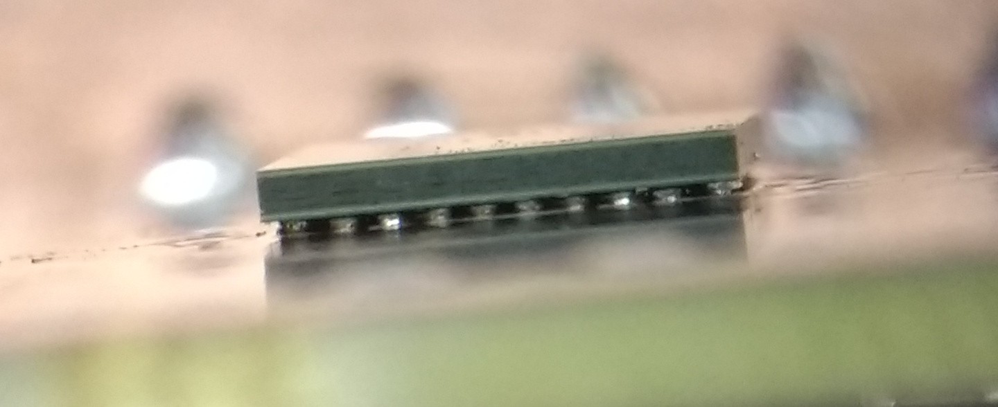
I haven't tested it yet, other than applying power and looking for smoke (none was forthcoming), but the outside ring looks OK from all four sides. This is much better than the first time, when half of the balls were bridged. Here's what happened:
1. I populated the other side of the PCB first
2. I applied a low-temp bismuth-based solder paste to the BGA pads on the PCB. I used too much, although I figured it would just get pulled to the right places during reflow, like it does with other packages. This was a mistake.
3. I reflowed the part with hot air. Afterwards, there were a lot of bridges between balls visible.
4. I removed the part with hot air, cleaned off the PCB with solder wick and flux, and manually repaired the solder balls on the part as best I could.
5. I applied just flux to the PCB (no paste), then reflowed the part on with hot air. It kind of looks OK, and didn't blow up with power applied, so maybe it'll work.
When I populate the next one, I'm just going to use a tiny bit of solder paste. I'm tempted to just flux the board and use just the solder balls on the part.
In any case, here's the front side of the PCB:
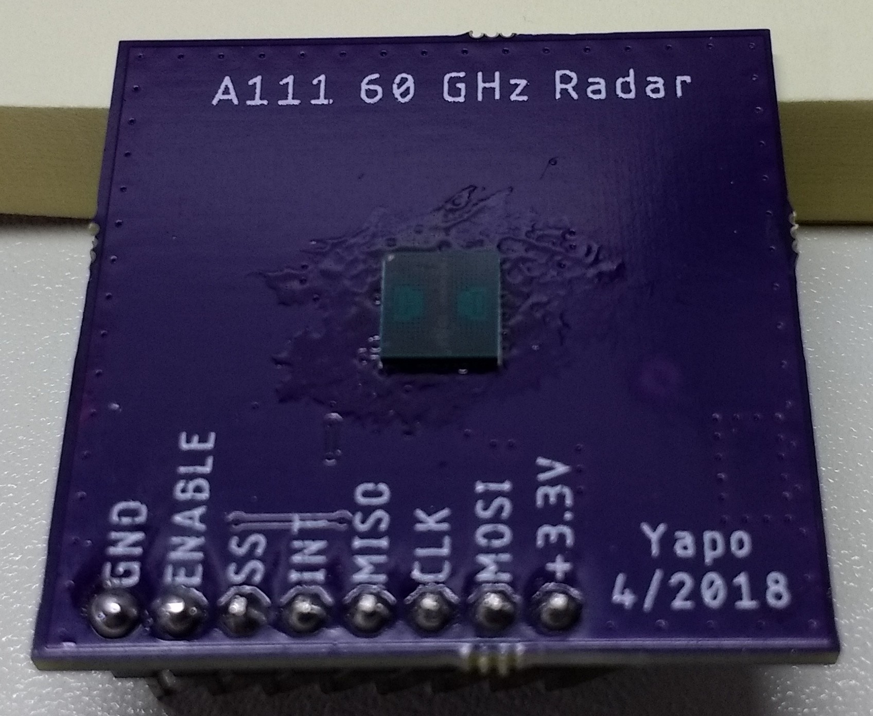
and the back:
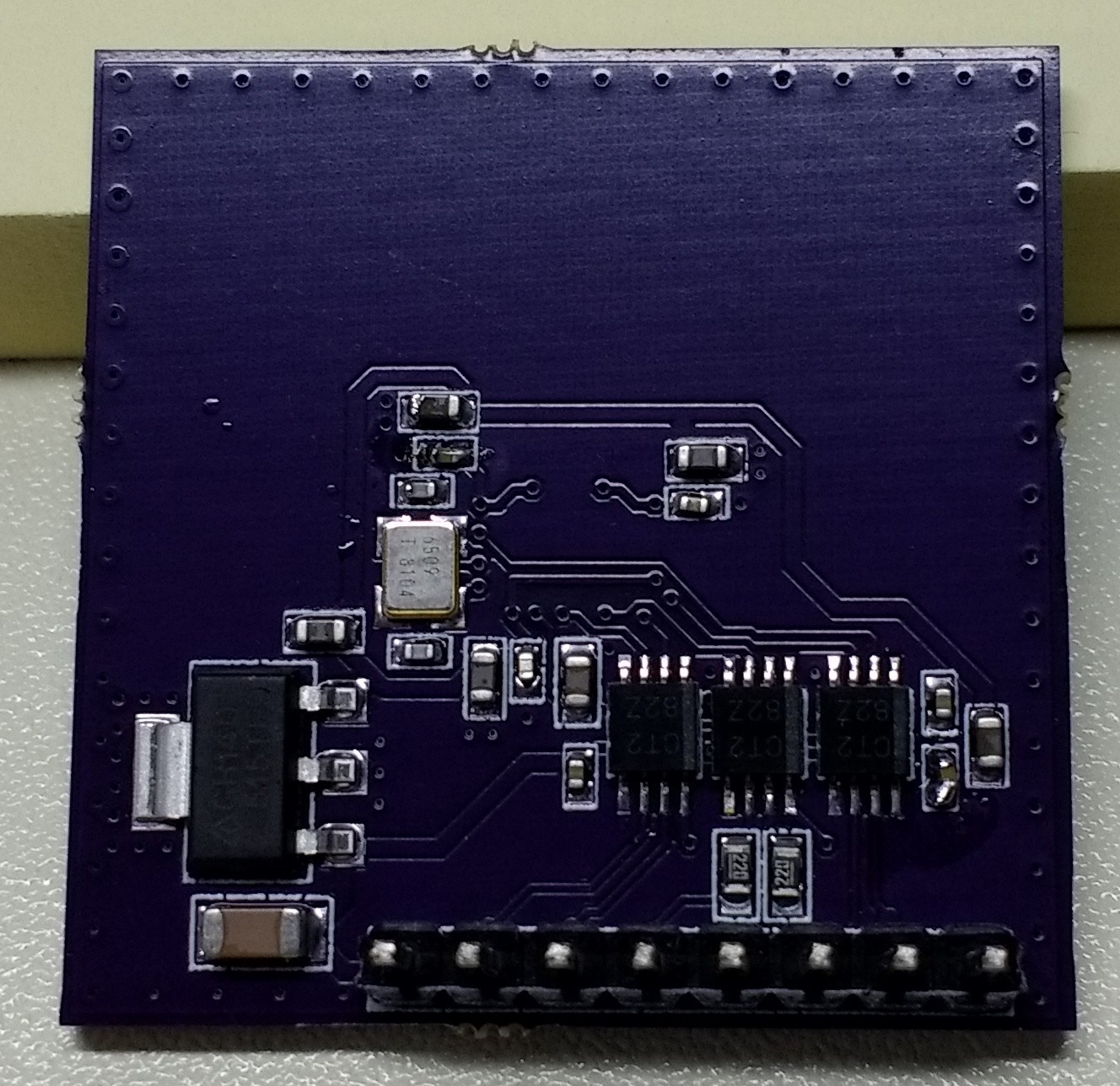
Some of the 0402 caps tombstoned on me for some reason, and I had to manually re-solder them. My solder paste is very old, so maybe it's not up to the task - I can try pre-fluxing the PCB with the next one to see if that helps.
Finally, here's a close-up of the radar part:
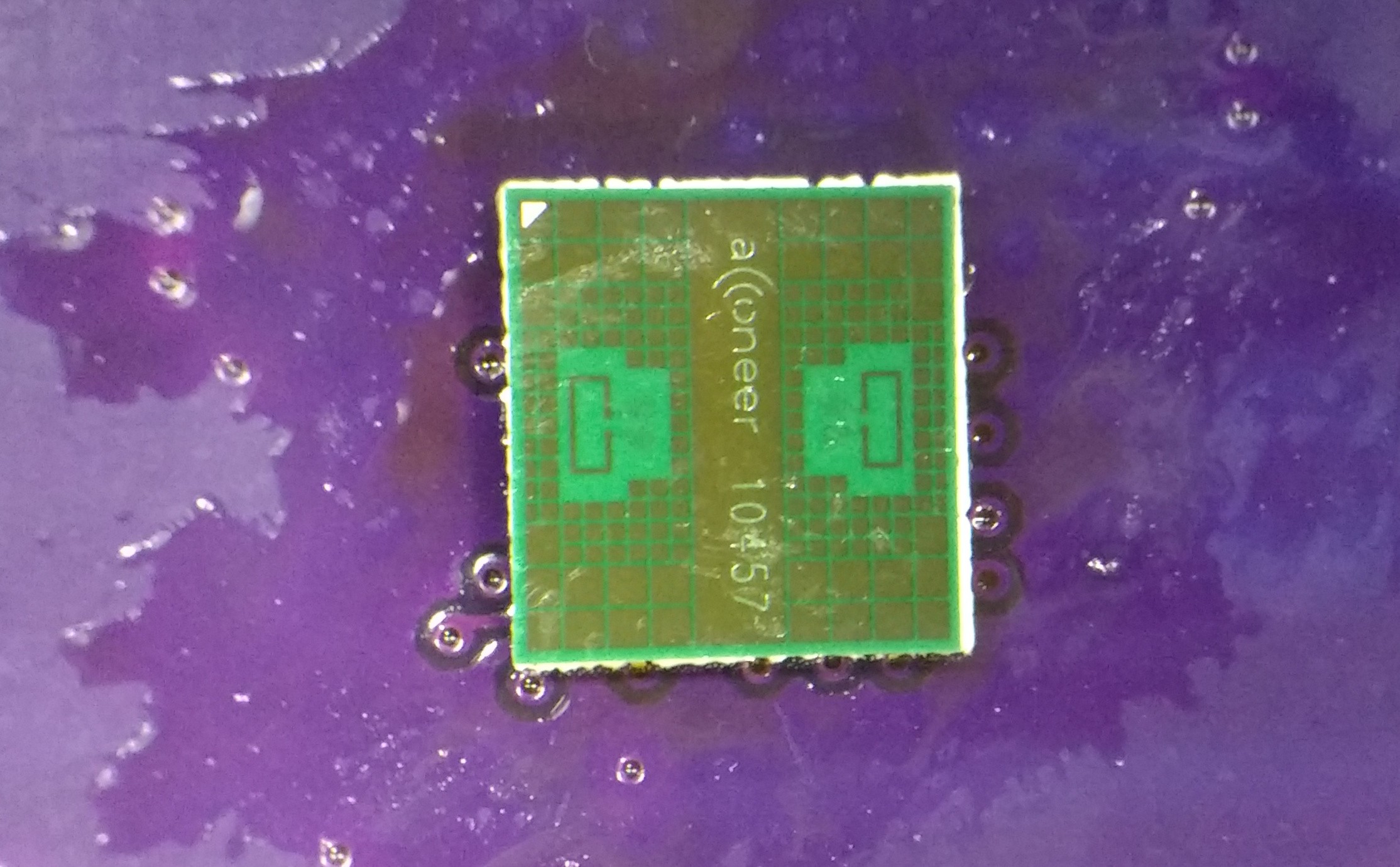
You can see the little antennas - presumably one for TX and the other for RX, but I have to be careful. In order to get access to the closed-source binary-only firmware for the part, I had to agree not to reverse engineer it. Is recognizing antennas and counting them reverse engineering? Oh, but I'm getting ahead of myself. I was going to save the licensing rant for its own log...
Discussions
Become a Hackaday.io Member
Create an account to leave a comment. Already have an account? Log In.
BTW I use the ESD protection diode to check for connectivity. i.e. the grounding diode by connecting the red DMM probe to ground and the Black one on each signal. Yes I intentionally reverse the probes to trigger the protection diodes. Using the diode test, I test the connections to the BGA. Only BGA I tried was a 4x3 CSP part in 0.4mm. Chinese HASL with large mask aperture with flux actually works better for me. If only they align their solder mask better. :(
https://cdn.hackaday.io/images/8270911437835915217.png
https://cdn.hackaday.io/images/8538981430578994241.jpg
Are you sure? yes | no
That's a neat idea, and much easier than building my own x-ray :-)
Unfortunately, on this PCB, I have fine-pitched parts (the level translators) on the other side that I reflow first, so their protection diodes would be in parallel with the ones on the DUT. I could hand-solder the translators after the BGA is mounted, but that's likely to be frustrating as well.
Are you sure? yes | no
That idea came from TI's app. note for using protection diode as a on-die temperature sensor for DUT.
Are you sure? yes | no
I proposed testing the ground diode because it has good coverage on all I/O types (that are ground referenced) under most situations. (There are weird ELC, PECL, that might not work.)
There is also the protection diode to the supply rail that you could try on DUT. External level shifting chips would have a different input structure (e.g. Zener diode) that allows for 5V tolerant and won't interfere with the test. Even if they do (unlikely), it would clamp to the higher I/O that you are shifting to.
This obviously won't work if the DUT uses a lower I/O rail that is internally generally generated and not available outside or that itself has higher I/O tolerant.
Are you sure? yes | no
@K.C. Lee I guess I could also heat the DUT with a little hot air while testing the protection diodes. This should reduce the forward drop to less than the room-temperature ones in the translators, so I should be able to "see" them separately.
Are you sure? yes | no
I have found that 27 guage syringes and quikchip SnBi solder paste (low temperature solder paste) can handle the scariest BGAs and WLCSPs with a little practice. It might seem obvious but the trick is two fold. Most important is to just cover the metal pad with solder paste with solder mask showing between adjacent pads. This prevents the majority of bridging probems. My rule, if the solder paste is touching at room temperature, bridging is likely. The second trick is proper placement. This can be tricky if relying on silkscreen frames/markers to position parts like I do since there is often an unintended offset between component pads and silkscreen from the fab (because the fabs are run by evil people, evil I say!). With low temperature solder paste, the components are less likely to "wick into place" as at high temperatures and proper placement avoids a host of ills, especially with components whose leads you can't see.
My recommendation is that you start with a new pcb and before doing anything else spend some time placing the solder on the BGA pads, wipe and repeat until you can control where it goes. This is more than half the battle. Nice, little uniformly-spaced islands of solder paste covering most if not all of the metal pads is the goal, and in an afternoon you will be master of the solder paste!
Good luck...
Are you sure? yes | no
Thanks! I did use a 27 ga needle, but was a bit heavy-handed with the paste. I knew there was too much glopped on there, but didn't take the time to wipe it down and start over. Having never done it before, I didn't know how precise you need to be - I guess I got spoiled because solder paste seems to do magic with most SMT parts - slap some down nearby, and surface tension does the rest.
I have two more PCBs and two more parts ($12 each), so I get a couple more tries. For all I know this one will work, and it's just a matter of making the process less painful for the next ones...I'll know soon enough.
Now I wonder if there's enough electrical conductivity with just the un-cooked paste to make a simple electrical go/no-go test before reflow to verify alignment. Maybe using some version of the protection-diode trick @K.C. Lee mentions above?
Are you sure? yes | no