Close
0%
0%

8 Bit TTA Interpreter

TTA (Transport Triggered Architecture) is very simple CPU type.

Similar projects worth following
The Weird CPU is an 8 bit TTA (https://hackaday.io/project/12879-weird-cpu). It has a binary front panel, used for programming and program display. It has an 8 bit wide data bus and an 8 bit wide address bus. This limits the CPU to 128 bytes of ROM for the monitor, 120 bytes of RAM for the program. The other 8 bytes is for the embedded hardware (i.e. the ALU, PC and I/O registers). This project looks at the development of an "interpreter" for the TTA architecture.

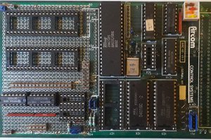
The Weird CPU (TTA8)

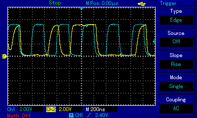
Here is my 8 bit Weird CPU  (https://hackaday.io/project/12879-weird-cpu) in action (playing LED Light Chaser):

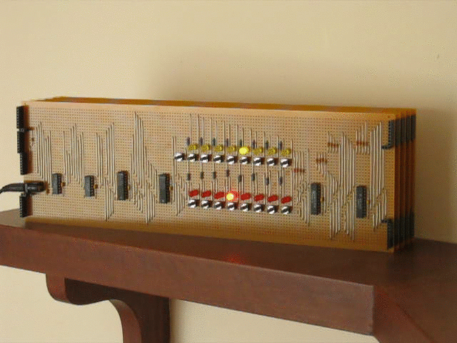
When programming, the bottom (red) LEDs are for the memory address entry, and the top (yellow) are for data entry. The extra switch on the left of the top row is the reset button.

Micro-Code and Micro-Programming

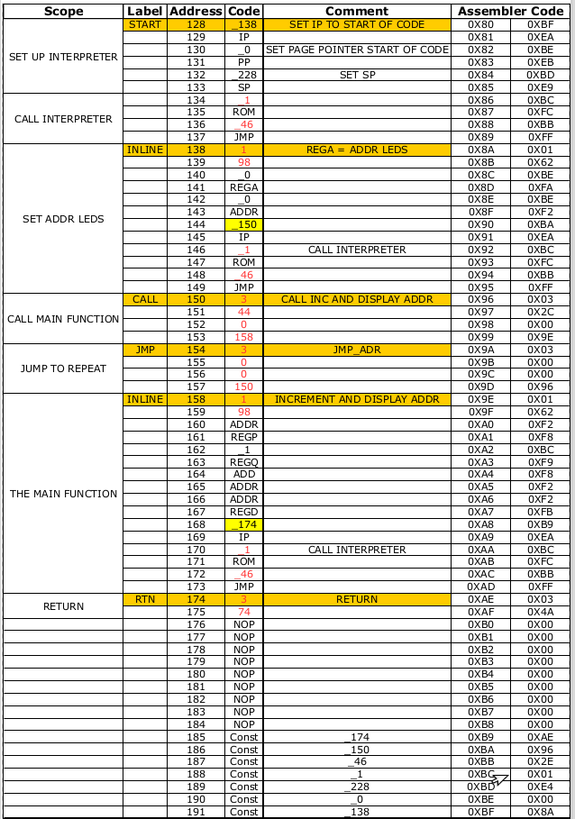
The TTA8 instruction set is very minimal:

  • Move Fetch_Address to Deposit_Address

With the Input/Output (I/O), Program Counter (PC) and ALU embedded in the address space, we also have:

  • Unconditional Jump
  • Jump On Carry
  • ADD
  • NAND
  • Input/Output

The input/output registers (REGA and REGD) are used by the Front Panel.

The TTA8 native instruction set is not very OpCode like, that is why the CPU is called Weird! The native instruction is It is best described as micro-code. And coding micro-code is often called micro-programming.

The major limitation for the TTA architecture is that the code density is very low. It takes a lot of instructions (or a lot of hardware) to do anything useful. The purpose of an interpreter is the increase the code density, to make the code look move conventional or OpCode like. The cost of this is execution speed.

The TTA8 just does not have enough memory (without paging) to develop a serious interpreter, but the code developed will run on a 16 bit TTA (TTA16) providing the architecture is similar. So it makes a good test bed to get an idea of what is possible.

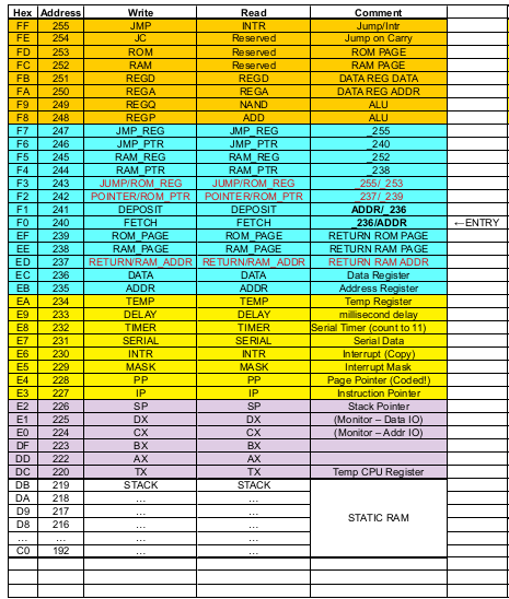
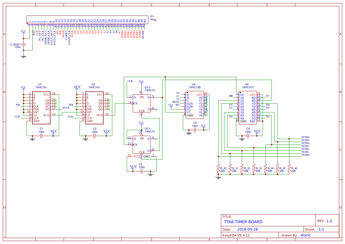
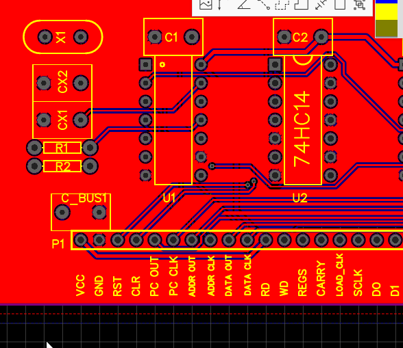
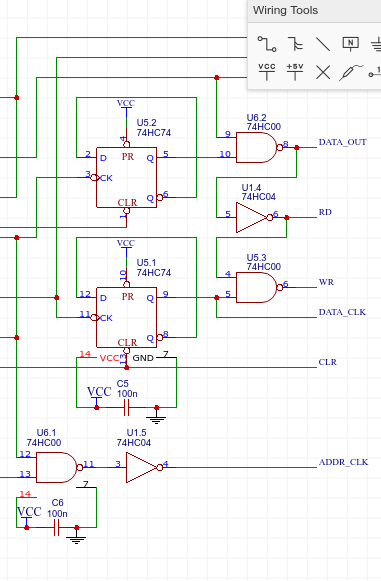
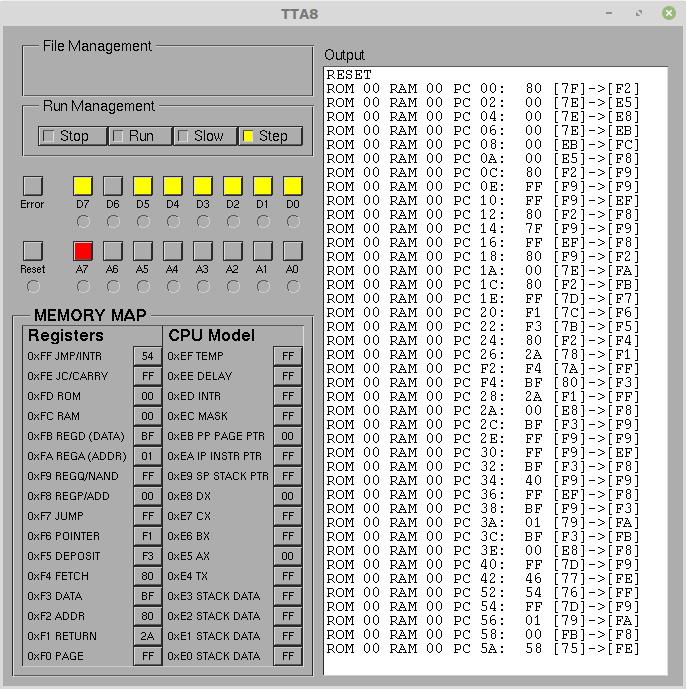
Proposed Memory Mapping

Here is the basic memory map of the TTA8:

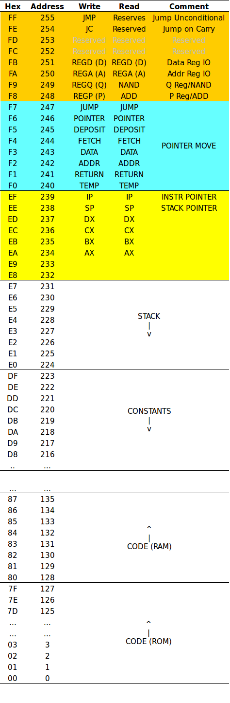
Starting from the top:

  • Hardware registers:
    • Unconditional jump
    • Jump on carry
    • Front panel data register (I/O)
    • Front panel address register (I/O)
    • ALU: Q register (write) or NAND register (read)
    • ALU: P register (write) or ADD register (read)
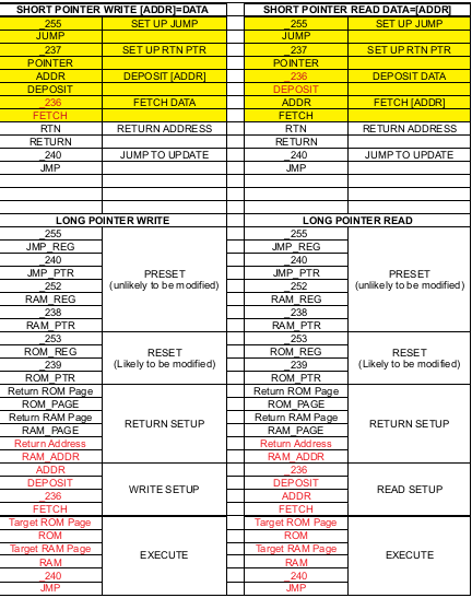
  • Indirect addressing (i.e. pointer move)
    • The TTA architecture uses self-modifying code for indirect addressing
  • CPU Model:
    • Instruction Pointer (IP)
    • Stack Pointer (SP)
    • Other registers (proposed)
  • Stack
  • Program constants
  • Program code (ROM)
  • Monitor code (ROM)

The Interpreter

An interpreter allows the CPU to emulate OpCodes and there by increase the code density. The cost to this is speed. An interpreter is very roughly 10 times slower than native code. Actually it is much slower because the Interpreter has other house keeping duties, such as managing the Interrupts.

Update

After many months of working on this project it is time to de-clutter.

AlanX

spreadsheet - 122.44 kB - 04/07/2019 at 13:45

Download

- 82.02 kB - 04/07/2019 at 13:45

Download

x-msvideo - 2.73 MB - 04/02/2019 at 03:35

Download

Adobe Portable Document Format - 2.14 MB - 03/23/2019 at 05:41

Preview
Download

TTA8.fd

The XForms fdesign file

- 47.27 kB - 03/19/2019 at 01:33

Download

View all 10 files

  • Reboot

    agp.cooper09/14/2019 at 07:10 0 comments

    Reboot

    Sometimes a project gets "long in the tooth" with no clear exit point.

    In many respects I am at this point. Progress is very slow. The exit point is far away.

    To reboot you need a new way?

    I was looking at my SubLEq compiler and I realised that of the two huge faults: low code density and low speed, I could have fixed low code density by using a library rather than direct SubLEq code. That is just substituting OpCodes with SubLEq code.

    With that in mind looking at my PL/0 compiler, it produces P-Code (27 primitives) that is converted into OpCodes (35 primitives), it struck me that 35 primitives for the TTA8 is quite doable.

    PL/0?

    PL/0 is a Pascal like language written by Niklaus Wirth. I have ported his code to C and extended the capability of the original code.

    Here is an example of PL/0:

    { Program Test String }
    (* Program Test String *)
    /* Program Test String */
    // Program Test String
    
    const true=1,false=0;
    const min=-2147483648;
    var Str[12],Msg[12];
    
      procedure ReadStr;
      var i,test;
      { Read a Pascal string, uses Str }
      begin 
        i:=1;
        test:=true;
        while test=true do begin
          getc Str[i];
          if Str[i]<32 then begin
            Str:=i-1; { Str == Str[0] }
            test:=false
          end else begin
            if i=12 then begin
              Str:=i
            end else begin
              i:=i+1
            end
          end
        end
      end;
    
      procedure WriteStr;
      var i;
      { Write a string, uses Str }
      begin
        i:=1;
        while i<=Str do begin
          putc Str[i];
          i:=i+1
        end
      end;
    
      procedure WriteMsg;
      var i;
      { Write Msg }
      begin
        i:=1;
        while i<=Msg do begin
          putc Msg[i];
          i:=i+1
        end
      end;
    
    begin
      Msg:="String Test";
      call WriteMsg;
      putc 10; { new line }
    
      Msg:="Enter str: ";
      call WriteMsg;
      call ReadStr;
    
      Msg:="You wrote: ";
      call WriteMsg;
      call WriteStr;
      putc 10; { new line }
      putc 10; { new line }
    
    end.
    // End Program Test String

     And the run:

    Begin PL/0:
    
    String Test
    Enter str: Hello World
    You wrote: Hello World
    
    End PL/0.

    Why PL/0? Really it could be any simple P-Code compiler. I just have this one on hand. I would most likely upgrade to a C like compiler in the future.

    So what are the OpCode primitives:

    // CPU model 16 bit
    • int Ax;                 // Primary Register
    • int Bx;                 // Secondary Register
    • int Tx;                 // Temporary Register
    • int PC;                 // Program counter
    • int SP;                 // Stack pointer
    • int BP;                 // Base pointer (base of active stack)
    // OpCodes
    • pushAx() {SP--;stack[SP]=Ax;}
    • popAx() {Ax=stack[SP];SP++;}
    • popBx() {Bx=stack[SP];SP++;}
    • subAxBx() {Ax=Ax-Bx;}
    • addAxBx() {Ax=Ax+Bx;}
    • mulAxBx() {Ax=Ax*Bx;}
    • divAxBx() {if (Bx!=0) {Ax=Ax/Bx;} else {Ax=min;}}
    • modAxBx() {if (Bx!=0) {Ax=Ax%Bx;} else {Ax=min;}}
    • oddAx() {Ax=Ax&1;}
    • eqAxBx() {Ax=(Ax==Bx)?1:0;}
    • ltAxBx() {Ax=(Ax<Bx)?1:0;}
    • leAxBx() {Ax=(Ax<=Bx)?1:0;}
    • neAxBx() {Ax=(Ax!=Bx)?1:0;}
    • gtAxBx() {Ax=(Ax>Bx)?1:0;}
    • geAxBx() {Ax=(Ax>=Bx)?1:0;}
    • movAxBx() {Ax=Bx;}
    • movTxAx() {Tx=Ax;}
    • movBxTx() {Bx=Tx;}
    • movBxImm() {Bx=Operand[PC-1];}
    • jmp() {PC=Operand[PC-1];}
    • jz() {if (Ax==0) PC=Operand[PC-1];}
    • movPCAx() {PC=Ax;}
    • movAxPC() {Ax=PC;}
    • movAxSP() {Ax=SP;}
    • movSPAx() {SP=Ax;}
    • movAxBP() {Ax=BP;}
    • movBPAx() {BP=Ax;}
    • decAx() {Ax--;}
    • incAx() {Ax++;}
    • movAxIndirectAx() {Ax=stack[Ax];}
    • movIndirectAxBx() {stack[Ax]=Bx;}
    // System
    • write() {write(Ax);}  // Put int
    • putC() {putc(Ax);}   // Put char
    • read() {read(Ax);}   // Read int
    • getC() {Ax=(int)ch;} // Get char
    • // Hidden Primitives...
    Read more »

  • Update After A Long Pause

    agp.cooper09/02/2019 at 07:02 0 comments

    Update

    I rebuilt the paged memory board and the Flash Programmer for a ZIF socket. It allows quick and easy Firmware updates.

    Other than a initial glitches for the Flash Programmer (probably still wet from the solder flux solvent), it all works.

    Now Where Was I?!

    After a long break I have to work out where I was:

    Current firmware:

    • TTA8_FlashProgrammerSDPv4a

    The Interpreter primitives coded:

    • inline 
    • call
    • jmp
    • jz
    • mov ax,[bx]
    • mov [bx],ax
    • push ax
    • pop ax
    • push bx
    • pop bx
    • xchg ax,bx
    • xchg ax,cx
    • xchg ax,dx
    • xchg ax,sp

    and:

    • jnz_timer
    • jz_sflag

    Load program has been coded:

    • 80 84
    • 81 FD
    • 82 85
    • 83 FF
    • 84 06 (ROM #)
    • 85 00

    Current programs include:

    1. Program 06 is an 8 Bit Counter
    2. Program 07 is a 16 Bit Counter
    3. Program 08 is Serial Echo

    Basically I remember I had to revert to this version of the firmware because I messed up the serial interrupt code. So I was working on the Interrupt and Serial code.

    Minor Firmware Updates

    Looking at how to read/write between RAM pages. I had made provision in the CPU model but had still to update the Interpreter. Done! Now the Interpreter updates the RAM_Page and ROM_Page registers when the ROM or RAM changes. Looking through my notes I see that I have written a standard for long pointer read/writes (i.e. between pages). Currently the Interpreter can only read/write inside a page. I need to move some code around to make room for long read/writes.

    I have this idea to move the Stack to a dedicated RAM page and to add a dedicated Return Stack (with its own RAM page).

    Checked the Serial I/O, it works fine.

    Updating the firmware is a very slow and repetitive process. I dare not do too much else I may not be able to debug the problem (been there!).

    So the next step is to migrate to long pointer read/write.

    Okay short and long read/writes done. Next is to move the Stack Pointer to its own RAM page.

    Undated the firmware for the new PUSH/POP/CALL/RTN code. Worked first off! Updated the EMU to confirm.

    New CPU Model

    Considering a closer approximation to the Intel 8080:

    • [IP] -> [PP][IP] (i.e. the Interpreter paged memory address)
    • [SP]->[RP][DP] (i.e. a return stack and a data stack)
    • [HX][LX]
    • [EX][DX]
    • [CX][BX]
    • [AX][FX] (i.e. A and Flags)
    • [TX]  (i.e. Temporary registers)

    With this in mind I have written MOV A,[C:B] and MOV [C:B],A type instructions where C is the Page and B is  the (RAM) Address.

    New CPU model updated. Test with default programs.

    Where am I going with this? I am thinking a tiny Forth. The Interpreter is basically an inner loop. So I need a number of primitives, a dictionary and the REPL.

    AlanX

  • One Step Forward and Two Step Back

    agp.cooper05/07/2019 at 12:43 0 comments

    One Step Forward and Two Steps Back

    Added the new Serial Card and the bus termination card, fired up the TTA8. The TTA8 built in test programs work but the system is a bit unstable. Unfortunately the serial port on my laptop did not work. Checked it with the old serial card, same problem. Checked Arduino and the same problem. Rebooted the laptop and the same problem.

    I had just got the laptop back from the repair shop! Okay, reset the permissions for the ports. Now it talks to the Arduino. Okay lets check the firmware for why the serial echo program did not work last time. Yes, found the problem, tried to recompile and the spreadsheet macro is missing! What happened to my laptop?

    Find an old version of the macro, as now I know that macros are stored in a configuration directory (and it is not there), they are not stored in the spreadsheet (nasty). Okay, update the macro for firmware changes. Updated the firmware. Fired up the TTA8. Erratic behaviour? Okay remove the bus termination card, that seems to have fixed it! Still the firmware is not 100% working as it should. This is going to take time to work out.

    Okay, find an old firmware that has a working serial echo program. Test it on the new serial card and success. Okay, the compiler will have to wait until tomorrow. I will take the win.

    Now I do not understand what happened to my laptop. How were the various security setting reset? Without the passwords the repair guy should not have been able to change anything even accidentally. Perhaps he reinstall Mint but kept the home directory. He does not need passwords for that. And it may also explain why I had to reinstall the "ezxdisp" library. A puzzle?!

    Okay I need to check the compiler and rebuild the firmware step by step to get back to where I was.

    A Puzzle Solved

    I now understand what happened. Because my laptop was out of action for so long (nearly two weeks) I forgot that I reinstalled Mint and was still in the process of setting it up.

    The problem with LibraCalc is that the macro is not stored in the "ods" file but in one of the  "~/.config/?" directories. So it was lost upon the reinstall. I did not back up the hidden files.

    AlanX

  • Firmware Upgrade Completed

    agp.cooper04/07/2019 at 09:38 0 comments

    Firmware Upgrade

    The TTA8 basically does not have OpCode like typical CPUs. It has a few micro-codes that are quite limited and rather difficult to use. The Interpreter reads "OpCode" and calls a subroutine. The CPU model is also simulated.

    The "Firmware Upgrade" as mostly about adding more registers to the System area. This unfortunately changes almost all of the existing register addresses. The reason was that I need more space near the top of memory for long pointer moves (to allow for writing to FRAM).

    Anyway, its done now. More registers will be added later but they will be below the System area and will not affect much.

    Serial IO Board

    Sent away a new Serial IO Board. Swapped out the 74HC93 for a 74HC161. The 74HC93 is rather rare nowadays (even though I have two spare).

    Serial Monitor

    The next firmware upgrade will be the addition of a serial monitor.

    ZIF Sockets

    I am definitely going to make a new programmer and Paged Memory Board with a ZIF sockets. I don't know why I have not done this so far. I suppose I never expected to need to reprogram the chips so many times.

    ---

    Termination Board

    Assembled the thermination board and added it to the back of the mother board.

    Not sure how to test it. Parhaps if I find and AM radio I can listen to the CPU noise with and without.

    Serial Board

    Assembled the new serial board.

    ZIF Sockets

    They don't fit, the holes are too small. I will have to redo the Programmer and the Paged Memory boards with larger holes.

    Coding

    Coding has stopped until I get my laptop back. It decide not to boot up one morming.

    AlanX

  • Adding the Serial Card

    agp.cooper04/03/2019 at 01:02 0 comments

    The Serial Card

    Well now I am getting excited! Okay not that excited as he chances of it working first time are practically zero. This card is complex and it is my first attempt at a serial design. What could go wrong!

    Here is the design:

     That big red line is a jumper I had to add as I forgot to craw it in the schematic and the PCB.

    Rereading the Schematic or What Did I Design!

    • U1-U5 decodes REGA and REGD and uses IO address 7 to read/write the serial data.
    • U6-U13 is the serial circuity.
    • U10.1 triggers INTR6 t0 indicates a byte has been received, and reset upon a read of the serial data.
    • U10.2 trigger the "serial in" clock on the "start bit".
    • Currently the serial interface is TTL but a current loop would be more "authentic".

     Okay, ready to code and "echo" program.

    No Surprise!

    Not surprised its not working. Working through the code:

    • MASK works
    • INTR works
    • ISR works
    • the Serial Card is holding INTR6 high?

    Ah yes, I have to do a dummy read to clear INTR6. It should have been cleared on RESET/CLR.

    Also I am not sure what happens on boot up  and clock reset.

    TXD in is indeterminate if disconnected.

    Need to add some RESET/CLR logic to the schematic.

    Not sure how Serial Out gets the clock signal? I have hooked it up to the Serial In clock that is triggered by the start bit.

    I think I may need to rework the schematic NOW.

    More Problems

    INTR6 can be reset by reading the serial data port. But better if it does not trigger on start up.

    The RX and TX signals have been swapped.

    And a 20ns glitch between the two 74HC165:

    The glitches are between D6, D7 and the two Marks. The data is "85" so D7 is wrong.

    D6, D7 and the Marks come from the second 74HC165 via QH and SER (serial in).

    I am puzzled by the glitches and D7 as the part of the schematic is a rather simple design.

    ---

    I ran with a different Interpreted program and get a different pattern.

    Yeah, I am writing new data at the baud rate (2.4kHz) rather than 1/10 or 1/11 of the baud rate.

    Need to add a dedicated counter to the Timer Interrupt.

    Success

    Well at least the the first test. Need to do a bit more to prove it (later as I have other chores to do today).

    • The test write 85 (i.e. 01010101 once every 12 timer interrupts (INTR7) to the serial port.
    • The test data (i.e. 85) is written to the ADDR LEDs.
    • The TXD is linked to RXD.
    • If INTR6 fires then the serial port is read (resetting INTR6).
    • The read data is written to the DATA LEDs.

    Okay a better test would be to write data to the ADDR and the show the read data on the DATA LEDs. I will do that later before ording a new Serial IO PCB Board.

    ---

    Time for a system rewrite, I need to make room for extra system variables (Serial Data, Timer Counter, etc), and provision for inter-page read/write. Here is the new system:

    Its getting complicated and I have to write notes on its use:

    I also want to shuffle the ROM pages around so that I can user the Monitor Run Program command to select a ROM page to run.

    ---

    Anyway, I have created a new Serial IO PCB board but I have to check on the availability or my stock of the 74HC93. Its pretty rare now so I should substitute.

    ---

    Really cool! Wrote some code to echo Serial In to Serial Out and to display the data on the front panel. Really cool after opening Putty to type stuff in the terminal to see the TTA8 echo it back and the front panel to display the character binary code (received and sent).

    So final checks on the replacement Serial IO Board before sending off for manufacture.

    AlanX

  • Adding the Interrupt Board

    agp.cooper04/02/2019 at 09:13 0 comments

    The Interrupt Board

    The Interrupt Board has three functions:

    1. read the interrupt inputs
    2. trigger an INTR7 every 417us (=2.4kHz)
    3. and provide the serial clock (SCLK=38.4kHz).

    Notes:

    • INTR7 is used as a timer.
    • INTR6 is the Serial In interrupt.
    • Interrupts are read every time the Interpreter is called.
    • Reading the interrupt register clears the interrupts so they are stored in "INTR".

    Interrupt Programming

    Recoded the Interpreter to call (if there are any interrupts) one ISR after another. Its up to the ISR to check if the interrupt is for it.

    As a test to check that the interrupts are actually being called, I wrote a short interpreted infinite loop. Then coded ISR7 to do a 16 bit binary count.

    Pretty cool actually. The concern is that interpreted code is much slower than expected and the interrupts timing is perhaps too fast. Roughly five interpreted OpCodes per interrupt.

    I may look at redesigning the interrupt card to slow it down.

    Otherwise good progress.

    AlanX

  • IC5 on the Control Board has retired!

    agp.cooper03/25/2019 at 01:53 2 comments

    Celebrated Too Soon

    After glowing with the success of getting the machine working, I modified the monitor and it stopped working! After a day of mucking around with monitor code, I thought I better check if the signals are working. Checked with the oscilloscope and they appeared to be there. Checked the address/data bus and it was not reading the FRAM correctly. Replaced the FRAM (no), cleaned the boards (no). Okay check the signals properly (yes), the Control Board is not working properly. I have blown up IC5? How?

    I will have to wait until the new boards arrive.

    16 bit counter demo code

    The new code has a 16 bit counter that will visually look better. I will post a video to prove that the machine is working!

    Next Steps

    Lot of things that could be done but writing some code to "save" and "load" a RAM page to FRAM sound like a good idea. Save recoding after each power up.

    After that setting up the Serial IO interrupt code seems like a nice (big) step.

    ---

    Saving code to FRAM is a bit tricky as FRAM is not available while being programmed.

    So I need to load a program into "static" memory (0xC0 to 0xDF), not much to play with.

    It is possible to swap between RAM pages, if necessary.

    Anyway so I wrote some code to load from FRAM to RAM (0x80 to 0xBF), and auto-execute. At least I don't have to toggle code into the front panel anymore (other than than the six byte to load the code).

    ---

    Uploaded the latest emulator code.

    ---

    Replace the Control Board. No success.

    The Paged Memory Board is reading rubbish but the FRAM read/write okay.

    So I will have replace this board as well.

    I am really surprised I destroyed two board with protective capacitors across every chip.

    It was not like I noticed a static discharge.

    Checked the ALU Board and it seems fine.

    Don't have a check for the PC Board.

    ---

    Refreshed my memory with the inner workings of the Interpreter.

    Wrote a number of OpCodes:

    • _Delay(ms)
    • Mov AX,[BX] (current ROM/RAM Page only)
    • Mov [BX],AX (current RAM Page only)
    • Push AX
    • Push Bx
    • Pop AX
    • Pop BX
    • Xchg AX,BX
    • Xchg AX,CX
    • Xchg AX,DX
    ---

    Replaced the Paged Memory Board. All good the CPU is talking to me now.

    Used the front panel to input a 16 bit counter. Works fine.

    ---

    Although I coded ROM Page 6 with a loadable 16 bit counter I could not get it to work?

    It works on the emulator though.  Perhaps the FRAM does not have the latest code?

    ---

    The problem was that the Arduino Code was only set up to write 8 pages (4 ROM pages).

    I am up to ROM page 6! So easy fix. And guess what, the program load code works.

    All Good!

    AlanX 

  • Coding Errors

    agp.cooper03/19/2019 at 14:22 0 comments

    Coding Errors

    I seem to have been a bit careless keeping the most up to date monitor code.

    Whilst the emulator code is correct, the copy of the spreadsheet is not.

    I have mixed the address of the ROM Page and the RAM Page.

    The Flash Code is correct for Page 0, Page 2 and Page 3 but not Page 1 (but I have not got that far).

    Going though the Logic Analyser data I am getting incorrect reads (i.e. not equal to the Flash Code). This means:

    • I should look at slowing the clock down, and
    • improving the bus.

    Easy to check, I have a new Control card without the crystal installed.

    I can clock the CPU at 1kHz and see if it works.

    Improving the Bus

    I think this is really called bus terminations. Looking at the options I think I can add a card at the end of the mother board with something like the Bourns' RC termination (https://www.bourns.com/pdfs/rctermap.pdf):

    The values are:

    The typical bus impedance is in the order of 50 ohms.

    I designed the Bus Termination Board but before getting it made I thought I would look at the CPU signal on the oscilloscope. Now you may ask why not before, the reason is that it is quite hard to work out what you are looking at. Anyway I thought I knew what I was looking for now.

    Well I found no evidence of ring,all good except the data bus:

    Okay, the blue trace is the REGS signal (low is reading/writing to a register), the yellow trace is the data bus. Very sharp signals except for second last yellow pulse. This is very likely from the FRAM. The signal is delayed about 80 ns, not surprising as the FRAM is rated as 90 ns! Now the write pulse would be rising around the 100 ns mark, very close for comfort! Here is another:

    This time the FRAM is clearly too late. So okay, the problem appears to be a FRAM that is just too slow. So to test I need to lower the clock frequency.
    ---

    Found a 2.4576MHz crystal, added to the updated PCB I had made and assembled.

    Plugged it in and no! Checked the logic analyzer and the signals are wrong, what!

    Okay, logged on the EasyEDA and checked the schematic and PCB, checks out okay (according to the design manager). "RD" is not working so checked the schematic, looks okay. Checked the PCB and "VCC" is connected to "RD". That's not right. Unrouted the PCB and reran the router, same error. Log a bug report, may need to find another PCB supplier as you cannot afford this types or errors. But I will see what they say.

    Spent the morning tracking the error, back to the schematic and to U5.3 pin 4.

    Here is the PCB error (VCC connected to RD, at the bottom):

    Here is the Schematic:

    Notice U5.3 should be U6.3! The problem is that pin 4 to U5.3 is connected to pin 4 for U5.2 which is linked to VCC! So my fault when I renumbered the ICs.

    Ordered a new control board and the bus termination board.

    Partial Success

    The code advances past the key check before failing. That means the jump to ROM Page 1 works. I checked the emulator and I was getting write to ROM in this area. The fault was "NOP", I had coded this as read/write address 0x00, a ROM address. A write to FRAM will cause write cycle but will not actually write the data. Not good as this means the FRAM will stop responding to normal reads. So I recoded "NOP" as read/write to 0xEF, the TEMP variable in RAM.

    So it boots up and allow me to read/write memory. The debounce does not seem to be working but I persisted and coded my binary counter. It works! Clocking LED D7 at about 7 Hz.

    It also does not boot properly on power up (the reset on the old control board?). But a manual reset works.

    So A good morning's work. Need to look at the Reset circuity and the monitor debounce code....

    Read more »

  • Port TTA8 EMU to XForms

    agp.cooper03/18/2019 at 06:55 0 comments

    TTA8 Status

    The machine is waiting for me to check why the latest card (Program Counter Board) did not work.

    But I thought I would port my old TTA8 EMU code to XForms. Not that easy as there are lots of buttons and labels to design and code. Here is current the form:

    I have hidden the file management buttons.

    These GUI programs get very big very quickly, in total 1200 lines of code so far.

    Speed wise it is slower than the original version and the output screen is a bit jerky when running fast, but it works fine.

    The built in "user" code is a binary counter, using the interpreter. The interpreted instructions are: Call, Jmp, Inline (i.e. native micro-code) and Rtn:

    Now that I have written a compiler that is suitable for this machine, so I now have the PCodes I need to "micro-code" for the interpreter (if that makes sense!).

    Its all a tight fit for an 8 bit CPU with an 8 bit address space (even with paging).

    For the "shell" I an considering my cut down version of "Mouse" with the ability to call ROM programs.

    But need to get the machine working first.

    I have uploaded the EMU_GUI project.

    AlanX

  • Almost Working

    agp.cooper03/04/2019 at 23:24 0 comments

    Almost Working

    Updated and tested the Software Data Protection version on the FRAM programmer.

    I had set my self a trap! "A14" is not set using SetAddr(), It has its own routine. But it is working now. I have uploaded the code.

    Endless Loop

    I also wrote a Control Card simulation so I could test the bus. Surprisingly the CPU is mostly working before going into an endless loop.

    It fails when I try to change the ROM Page. It should wait until a jump before changing the Page but it changes the Page immediately.

    It seems as if the LOAD signal (which signals the PC to jump on the next clock) is glitched.

    Using the logic analyzer I did (once) get it to show glitches every write machine cycle.

    How to fix?

    Cross-talk on the CLR Signal

    I am getting about 5 clock cycles on the CLR signal as the Reset triggers reset schmitt trigger. It does not appear to affect (but there is some evidence that it does!) the control circuit. It could be internal cross-talk (as the clock and reset circuity share the same chip) or external cross-talk because the components are close together.

    I am thinking of adding a 47 pF capacitor to the input gate of the reset logic.

    Next time I will use a 74HC14 rather than build my own Schmitt trigger.

    ---

    The capacitors did not work.

    Redesigned the clock and reset circuity.

    Redesigned the load signal to avoid the glitch areas between the machine cycles.

    Redesigned the boards and sent them off to be made.

    Bugger no sooner than I sent the order off I found an error.

    Oh well, I will sent the updated board tomorrow.

    I am getting close to working!

    AlanX 

View all 30 project logs

Enjoy this project?

Share

Discussions

Similar Projects

Does this project spark your interest?

Become a member to follow this project and never miss any updates