 agp.cooper
Coding Errors
I seem to have been a bit careless keeping the most up to date monitor code.
Whilst the emulator code is correct, the copy of the spreadsheet is not.
I have mixed the address of the ROM Page and the RAM Page.
The Flash Code is correct for Page 0, Page 2 and Page 3 but not Page 1 (but I have not got that far).
Going though the Logic Analyser data I am getting incorrect reads (i.e. not equal to the Flash Code). This means:
- I should look at slowing the clock down, and
- improving the bus.
Easy to check, I have a new Control card without the crystal installed.
I can clock the CPU at 1kHz and see if it works.
Improving the Bus
I think this is really called bus terminations. Looking at the options I think I can add a card at the end of the mother board with something like the Bourns' RC termination (https://www.bourns.com/pdfs/rctermap.pdf):
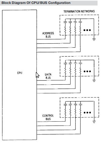
The values are:
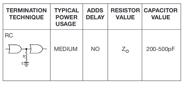
The typical bus impedance is in the order of 50 ohms.
I designed the Bus Termination Board but before getting it made I thought I would look at the CPU signal on the oscilloscope. Now you may ask why not before, the reason is that it is quite hard to work out what you are looking at. Anyway I thought I knew what I was looking for now.
Well I found no evidence of ring,all good except the data bus:
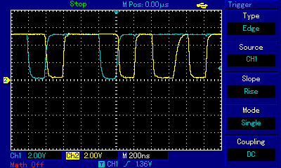
Okay, the blue trace is the REGS signal (low is reading/writing to a register), the yellow trace is the data bus. Very sharp signals except for second last yellow pulse. This is very likely from the FRAM. The signal is delayed about 80 ns, not surprising as the FRAM is rated as 90 ns! Now the write pulse would be rising around the 100 ns mark, very close for comfort! Here is another:
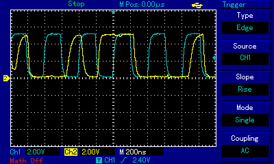
This time the FRAM is clearly too late. So okay, the problem appears to be a FRAM that is just too slow. So to test I need to lower the clock frequency.
---
Found a 2.4576MHz crystal, added to the updated PCB I had made and assembled.
Plugged it in and no! Checked the logic analyzer and the signals are wrong, what!
Okay, logged on the EasyEDA and checked the schematic and PCB, checks out okay (according to the design manager). "RD" is not working so checked the schematic, looks okay. Checked the PCB and "VCC" is connected to "RD". That's not right. Unrouted the PCB and reran the router, same error. Log a bug report, may need to find another PCB supplier as you cannot afford this types or errors. But I will see what they say.
Spent the morning tracking the error, back to the schematic and to U5.3 pin 4.
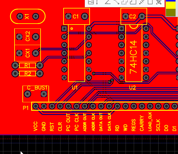
Here is the PCB error (VCC connected to RD, at the bottom):
Here is the Schematic:
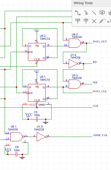
Notice U5.3 should be U6.3! The problem is that pin 4 to U5.3 is connected to pin 4 for U5.2 which is linked to VCC! So my fault when I renumbered the ICs.
Ordered a new control board and the bus termination board.
Partial Success
The code advances past the key check before failing. That means the jump to ROM Page 1 works. I checked the emulator and I was getting write to ROM in this area. The fault was "NOP", I had coded this as read/write address 0x00, a ROM address. A write to FRAM will cause write cycle but will not actually write the data. Not good as this means the FRAM will stop responding to normal reads. So I recoded "NOP" as read/write to 0xEF, the TEMP variable in RAM.
So it boots up and allow me to read/write memory. The debounce does not seem to be working but I persisted and coded my binary counter. It works! Clocking LED D7 at about 7 Hz.
It also does not boot properly on power up (the reset on the old control board?). But a manual reset works.
So A good morning's work. Need to look at the Reset circuity and the monitor debounce code.
---
Reworked the Monitor code to wait for debounce on the key press and the key release.
Had a bit of a code re-organise as well.
The emulator has been reworked to cope and prints the function names when called (makes it easier to follow the code).
Add a 2.2uF capacitor to the reset switch, I think the problem is that the power supply rises very slowly (by design?). I noticed this with this power supply previously.
So ready to burn the new monitor.
SUCCESS ALL WORKING!
AlanX
Discussions
Become a Hackaday.io Member
Create an account to leave a comment. Already have an account? Log In.