5/8/2018 Log #2 Power FETs
There might be a question for why do we need to use expensive, bulky and seemingly obnoxious external Power FETs. Well, if you want to deal with POWERful motors, and POWERful drives, rest assured the ONLY way, is with external FETs. Maybe when they come up with superconductors at room temperature will we be able to do high power H Bridges and Inverters in an integrated package. As it is today, however, if you want anything higher than 50W to 100W, there is no economical or practical way to package this in a small integrated driver.
Some of the applications we are dealing with here will source dozens of amps CONTINUOUSLY! This is not a "Yay! I saw a 20A pulse with a duration of 17 ns!" kind of deal. Oh no! This is more like "I will be pushing 20A to 30A for 5 minutes straight! And oh by the way, some of the spikes will be in the hundreds of Amps..."
I tell you, the only way is external FETs and with that come all other bunch of issues which must be dealt with. That is why it is so important to have the proper circuitry capable of dealing with all of these issues, and if you can package it all in a single device, even better! Here are some of the topics in question:
- The Pre Drive Stage. Although FETs can be turned on with TTL logic levels, this voltage is not enough to drive the FETs in an efficient manner. Ideally, you have a circuit which allows you to fully drive a FET ON so you can minimize its RDSON.
- Gate Drive Current. A FET will require a rather large current for a very small amount of time (in the few nanoseconds range). This is because the FET's gate is a capacitor. And also, because we want to turn the FET ON as soon as possible. The only way to overcome the FETs input capacitance is with a large current. Hence, we need the gate drive to have large current capabilities so we can both turn the FET ON and OFF at high speeds.
- High Side Driving. To form a Half H bridge you need a low side FET and a high side FET. The Low Side FET is the easy one to drive as you can use a low voltage with respect to GND to enable it. However, the high side FET can't benefit from this, as its source is floating. Traditionally, a P Channel FET would have been used, but P Channel FETs are expensive and not as common as N Channel FETs. We really want to use N Channel FETs due to cost constraints. The only way then, is to add some sort of circuitry which can generate the higher voltage to drive the high side FET gate.
- Dead Time. Whenever you have two FETs in series as in with a Half H bridge, it is of uttermost importance that a mechanism is put in place to ensure both of them are not enable at the same time. Having both FETs turn ON at the same time is quite catastrophic and we refer to this blunder as Shoot-Through. This is because for all practical purposes you have a short from the positive to the negative terminal, which as you can imagine can result in quite some large currents! Needless to say, shoot through will also result in the driver's destruction. Hence it's importance to limit at all costs. The solution is what is known as Dead Time insertion which is nothing else than a small delay in which we ensure the FET which was previously ON remains OFF before we enable the subsequent FET.
All of this circuitry can be implemented with discrete components or you could find packaged within a single device. With PAC52xx, it is merely one of the many included blocks. PAC52xx contains a Pre Drive stage suitable for driving the FET gates with 12V (15V for IGBT's). Depending on the device, the FET will see up to 2A worth of sink/source current to turn the FET ON and OFF as soon as possible. A Bootstrap topology gives us the ability to use N Channel FETs on both low and high side positions, which in turn provide cost savings and makes the system more robust thanks to RDSON optimization. And an internal and fully programmable dead time generator protects our application from deadly shoot through.
In the picture below I show the typical external FET implementation with a PAC5223 or PAC5232. This is for one leg of the Three Phase Inverter, so just multiply by three and you have the entire power stage.
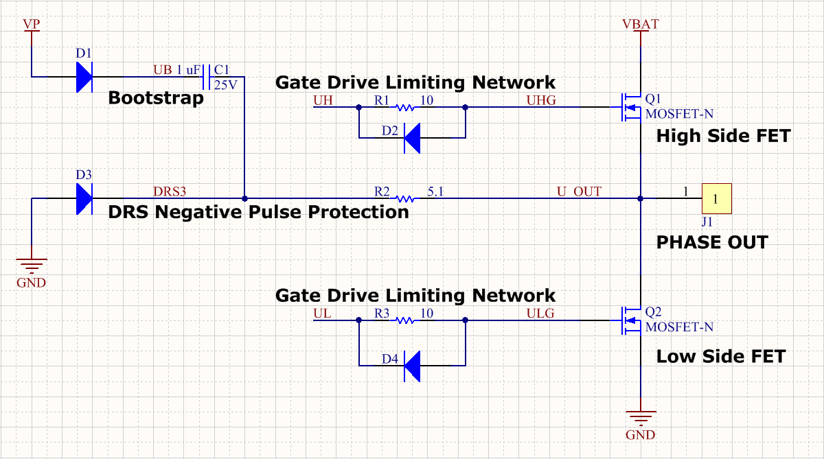
- D1 and C1 form the Bootstrap network. We need a bootstrap so the high side FET can see a VGS in the 12V range.
- D3 and R2 form a clamp to ensure the DRSx pin does not see too large negative voltage incursions which are prominent when switching large inductive loads/
- R1 and D2, as well as R3 and D4, are used to limit FET gate current. The resistors limit the current when turning the FET ON and the diodes open up a non resistive path when switching the FET OFF. Some people add a resistor in series with the diode.
- Q1 and Q2 are the N Channel Power MOSFETs. These should be rated for the Abs Max on VBAT and should be able to take on the current.
Discussions
Become a Hackaday.io Member
Create an account to leave a comment. Already have an account? Log In.