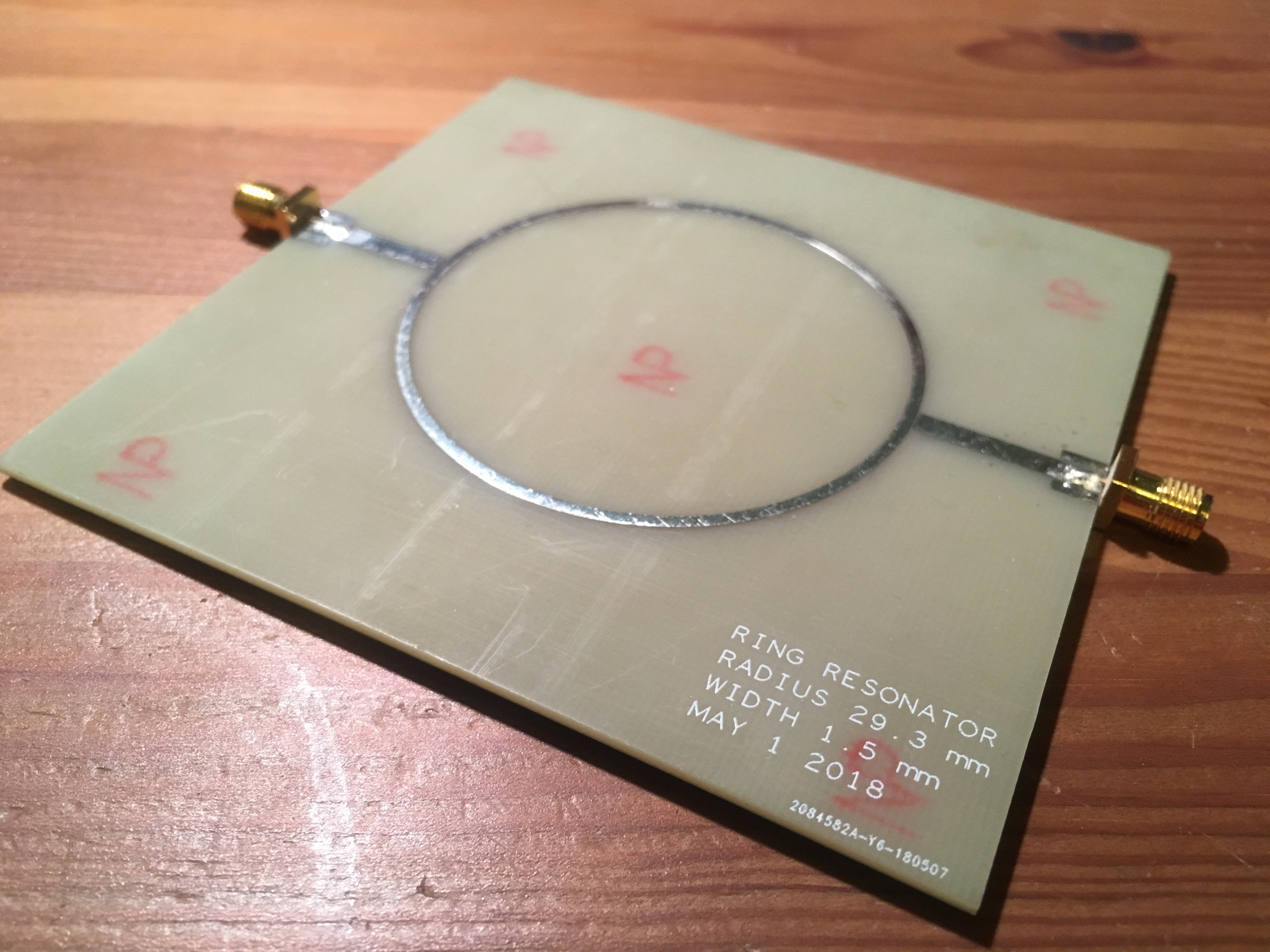
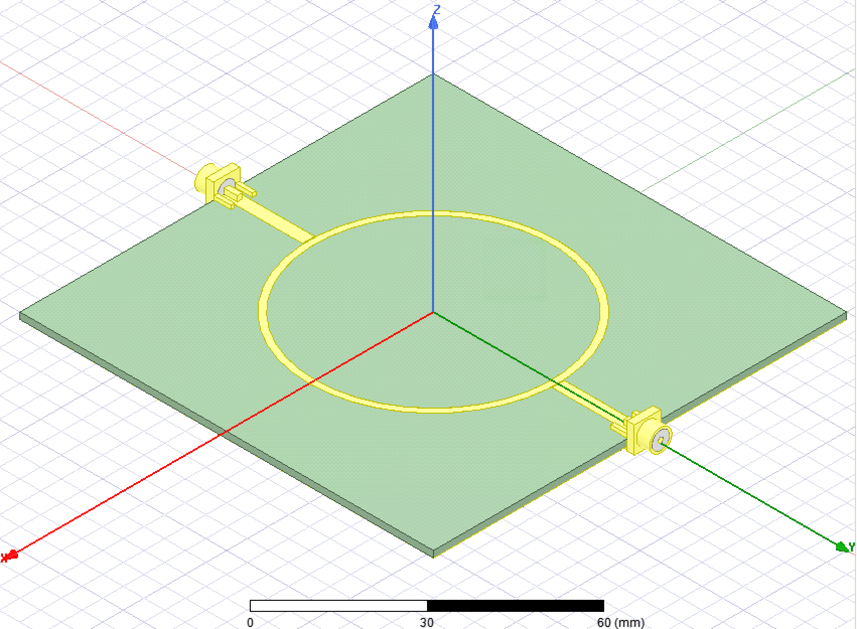
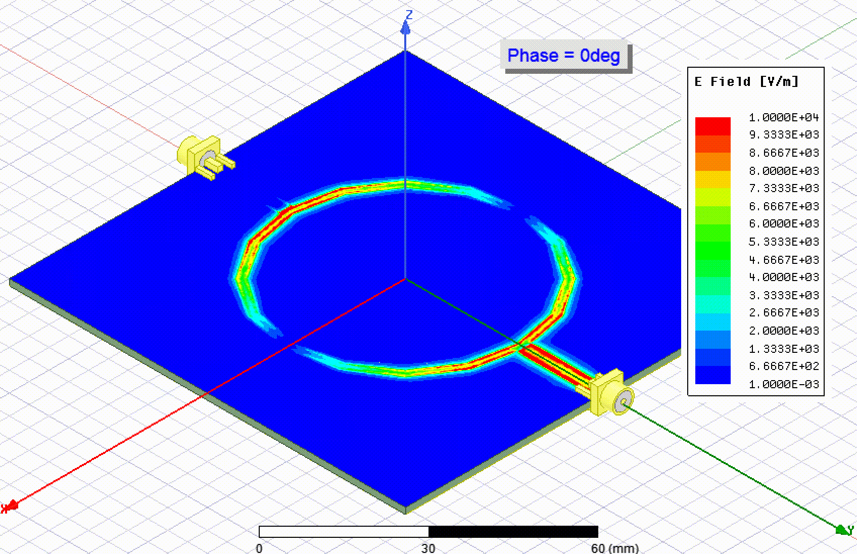
The cheap PCB fabricators don't have any sort of guarantees on impedance, which is part of the reason they are inexpensive. My thought is that if a specific impedance is required, you could fabricate this calibration structure, measure it, and use it to tweak your line width (or other geometry). Then order the PCB form the same supplier quickly and hope that the εᵣ is still the same. Or, you can fabricate it along with your PCB just out of curiosity as a way to check the εᵣ.
0%
0%
Measuring the Effective Permittivity of PCBs
Find out how you can measure the effective permittivity (a.k.a. dielectric constant) of your PCB substrate.
Become a Hackaday.io member
Already have an account? Log in.
Just one more thing
To make the experience fit your profile, pick a username and tell us what interests you.
Pick an awesome username
hackaday.io/
Your profile's URL: hackaday.io/username. Max 25 alphanumeric characters.
Pick a few interests
Projects that share your interests
People that share your interests

 Ted Yapo
 Michael Schembri
 MS-BOSS
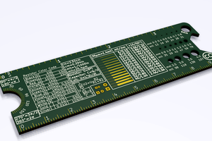
 Jan B.
Not to leave anyone hanging on that last comment; I found this paper which is the answer about loss tangent: https://aspocomp.com/wp-content/uploads/2020/03/Microstrip_ring_resonator_method160604.pdf
tl;dr Measure the loaded (Ql = frequency of peak / 3dB BW of peak) and unloaded Q (Ql / (1 - 10^(IL,dB/20))) of the resonator, use this to determine the alpha, and from that convert to Df.