Transmission lines like the microstrip are an essential ingredient in RF PCBs. The trace width required for a given characteristic impedance Z₀ can easily be calculated using online tools or KiCAD's calculator utility. One of the important parameters is the relative permittivity εᵣ of the substrate, also known as the dielectric constant. Companies that have cash often use expensive substrate materials that have a precise εᵣ over frequency and between lots, which means that they can be confident that the characteristic impedance will be consistent. Good PCB fabricators will also ensure that transmission line impedances are correct, but this is not the case with the cheap fabricators. Hobbyists usually rely on FR-4, which might have a relative permittivity anywhere between 4.35 and 4.8 (usually nominally taken as 4.4). That's a ±10% change, which would change a 50 Ω trace on a 1.6 mm PCB to 48 Ω at εᵣ = 4.8. That doesn't sound like much, and maybe it's OK. However, sometimes it is more critical.

What do you do if you need to know the relative permittivity of your substrate? There are many papers written on the topic, but I'm going to give the skinny on one of these, which involves measuring a ring resonator and some pretty straight-forward math. The details are laid out here, and you can also calculate the loss tangent, but I'm not going there so read the paper if you're interested!
Ring Resonators
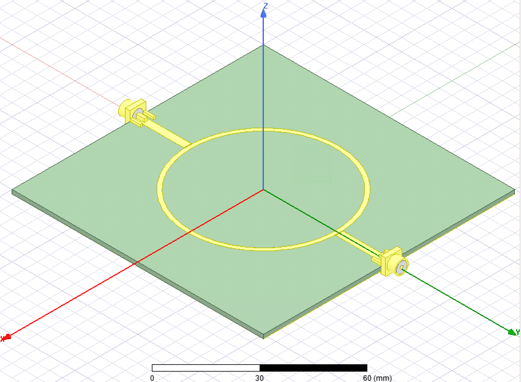
The ring resonator, shown below, is on a 10 cm x 10 cm PCB, making it cheap to fab ($2 at JLCPCB). The structure is a ring that is separated by a small gap to traces that lead to the SMA connectors. On the bottom there is a solid ground plane, so the traces are microstrip transmission lines.
To calculate the resonances of the ring, it can be thought of as being a straight line rather than a circle, which is appropriate if the width w of the line is much less than the radius r; this is called the "straight-line approximation". This article recommends that r/w > 7. At the resonant frequencies, there will be a standing wave, which mathematically requires that
Here, v is the phase velocity, c₀ is the speed of light, and εᵣ,eff is the effective relative permittivity. So we can measure the resonances and easily calculate εᵣ,eff. This in turn can be used to calculate the actual εᵣ of the substrate (e.g. FR-4) through a series of equations from various papers, nicely summarized here. These equations also capture the frequency-dependence. I have written a MATLAB program (in the files section of this project) that implements these calculations.
I was interested in measuring at 915 MHz in the ISM band, for which I calculated a radius of ~294 mm using a trace width of 1.5 mm and a 1.6 mm thick PCB. Unfortunately the PCB I sent to fab had a 293 mm radius that I found using some other calculations (which I believe are less accurate based on the simulations below). I made the microstrip lines from the SMA connectors 50 Ω since I will be measuring this with a VNA.
Simulation in HFSS
The coupling of the ring across the gaps can affect the resonance, so I was keen to simulate the resonator. I set up two models in HFSS, one with SMA connectors and one where the transmission lines were excited directly. To model the SMA connectors I followed this video on YouTube. As expected, the first resonance happened close to 915 MHz.
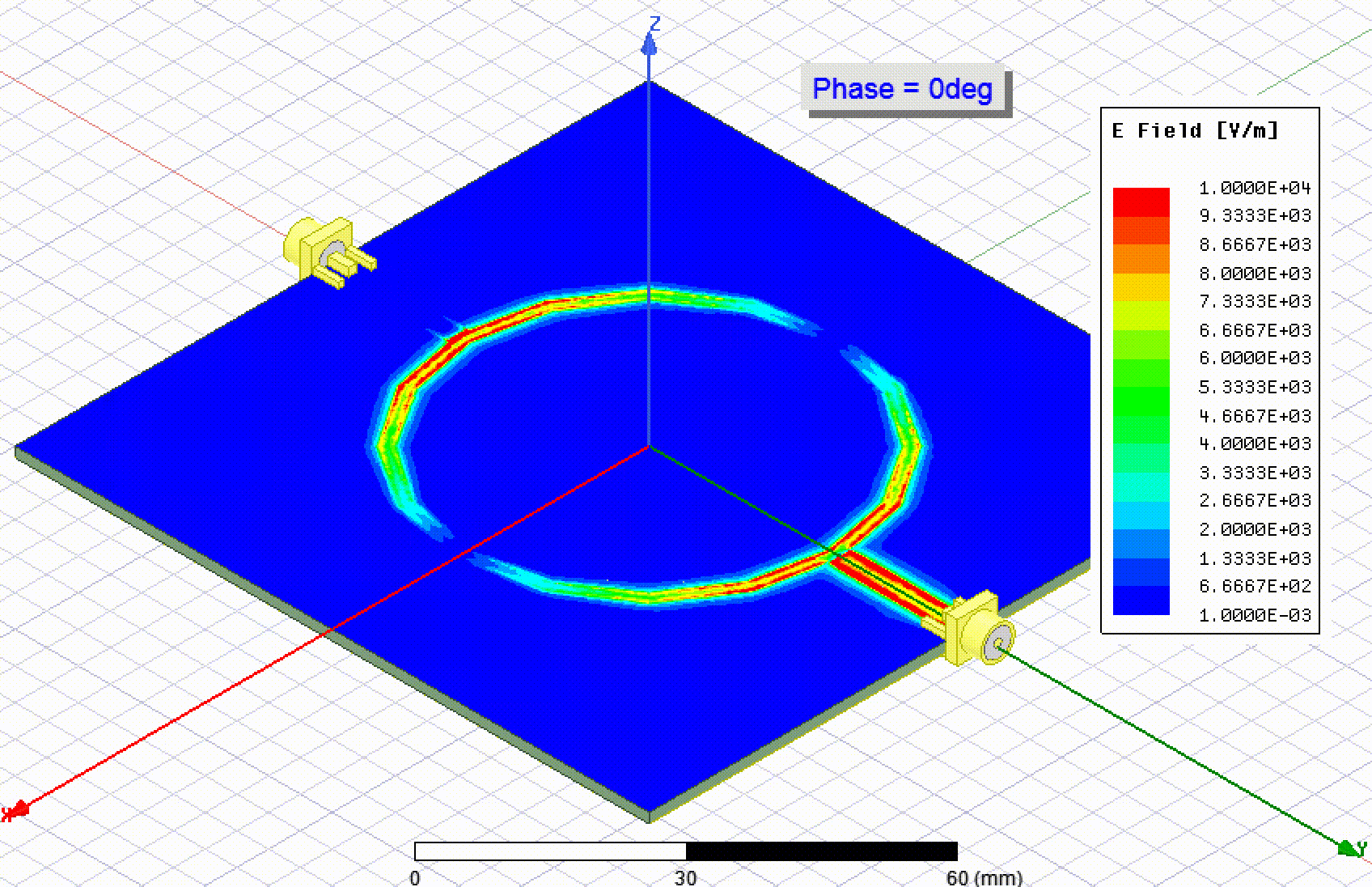
The second resonance is to be expected around 1830 MHz, which is the case:

As you can see not very much power is coupled through to the second port (in the animations, the closer port is excited). I mentioned concern about the loading of the ring due to the traces from the SMAs, so I did a sweep of the gap and plotted S21.

As expected, the smallest manufacturable gap of 0.16 mm couples the most power through. The resonant frequency also shifts lower as the gap is decreased. Note that the resonance is not exactly at 915 MHz because my ring has a radius that is slightly smaller than it should as mentioned earlier. This doesn't really matter though because using the equations from the MATLAB script, εᵣ can be calculated. I decided to use the smallest gap because the resonant frequency is closest to the correct value, and also the most power is coupled through.
Usually I use KiCAD but that unfortunately resulted in a dead end as it seems that KiCAD doesn't support anything but square geometry on copper layers. Thus, I used a trial version of OrCAD PCB Editor. I sent the gerbers to a fab and I'm excited to measure them!
Discussions
Become a Hackaday.io Member
Create an account to leave a comment. Already have an account? Log In.
At one point, I talked to one PCB supplier that work with Getek trying to figure out the dielectric variations over each layer of a stackup. Basically he told me that they only guarantee controlled impedance (by tweaking line width etc) and not control the dielectric constant.
Are you sure? yes | no
Yeah from what I hear the dielectric constant can vary a lot even between lots. The cheap PCB fabricators don't have any sort of guarantees on impedance. My thought is that if a specific impedance is required, you could fabricate this calibration structure, measure it, and use it to tweak your line width. Then order the PCB form the same supplier quickly and hope that the εᵣ is still the same. Or, you can fabricate it along with your PCB just out of curiosity as a way to check the εᵣ.
Are you sure? yes | no
Neither that PCB place nor the Getek (a specialized dielectric for high frequency ) are cheap. What I was asking for is on the *same* multilayer PCB what the variation would be. i.e. layer 1 vs layer 2 vs ... layer n. I wasn't even asking about batch to batch.
Basically there are less variation on the FR4 layers because it has a higher glass content than the preprep that have a higher epoxy content. BTW preprep are layers that goes between individual FR4 heat pressed to "glue" them together.
BTW if you look at new PC motherboard, you'll find out that all of them talk about the PCB weaves these days. The tighter weaves means that it is more uniform. (Not even care about moisture)
They make calibration coupons for figuring out the dielectric constants. Basically it is a set of transmission line that you can measure the impedance. The board maker use that to adjust their etch and line width. Some of their customers would also use that for TDR and S-parameter measurements.
FYI:
https://gigabytedaily.blogspot.ca/2011/08/gigabyte-ultra-durable-4-classic-new.html
Are you sure? yes | no