 J.B. Langston
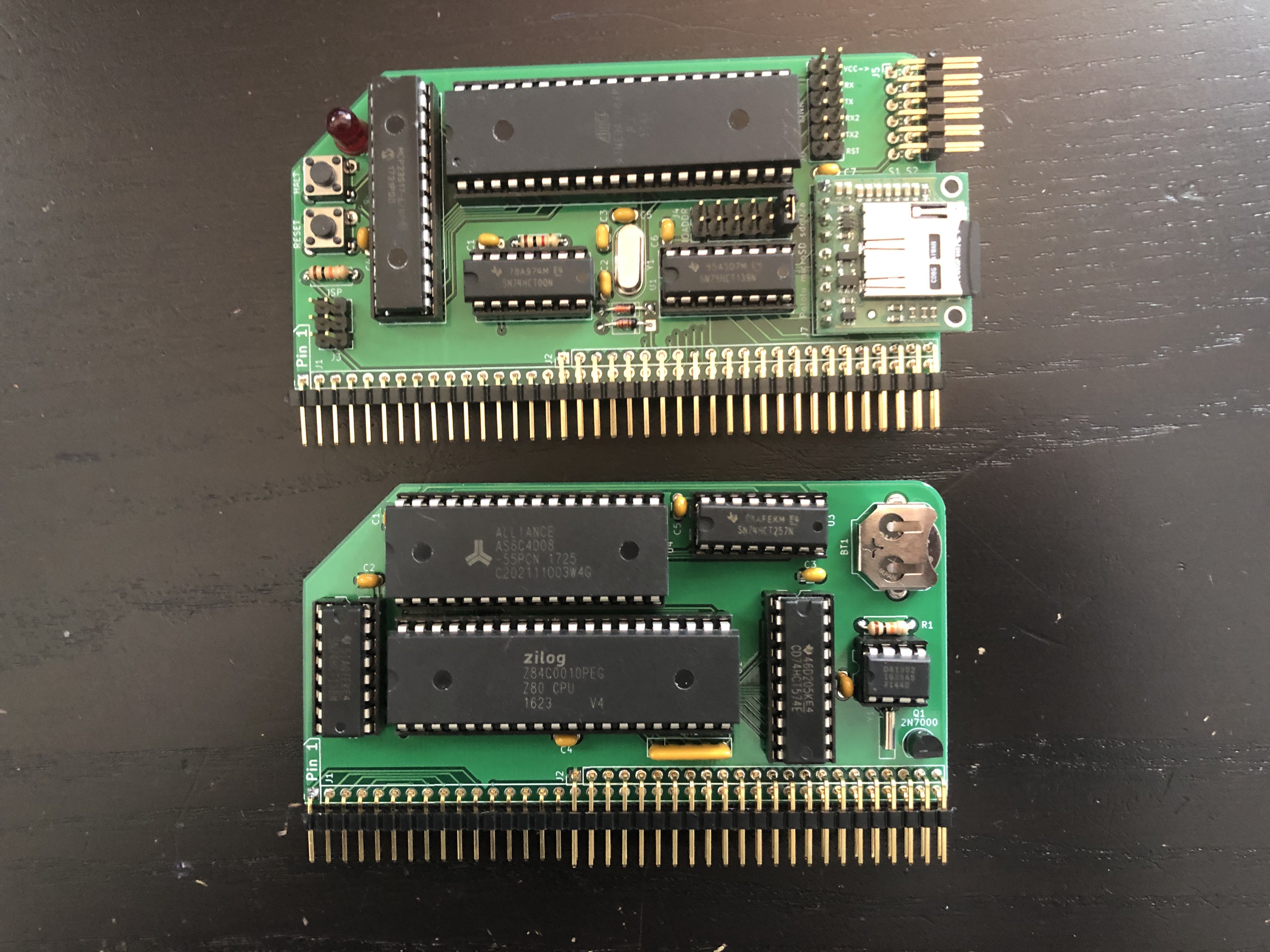
I've just put the final touches on a new revision of z80ctrl, plus a new companion module that combines a Z80 CPU, 512KB bankable RAM, and and RTC on a single board.
I expect kits for the new CPU board will be sold on Tindie and z80ctrl kits will be updated to Rev 6 once the current inventory of Rev 4 boards is sold out. The timing will be up to Michael Kamprath who is selling the kits. The current Rev 3 and Rev 4 boards will continue to be supported by the firmware, and the revision to build for will be configurable via a Makefile option.
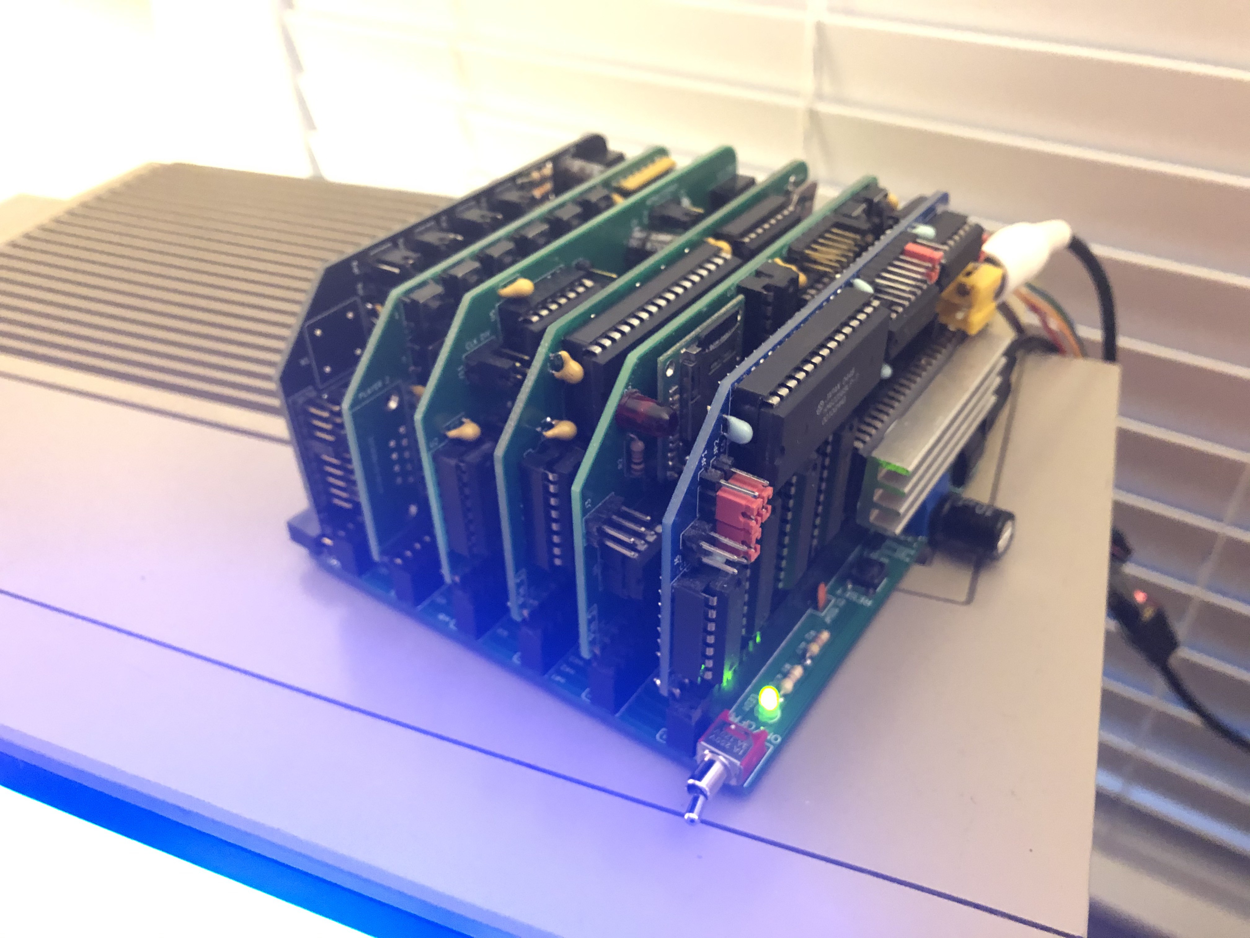
The z80ctrl plus the CPU board comprise a fully functional RC2014-compatible Z80 system in only two modules. The z80ctrl, CPU/RAM/RTC board, TMS9918 video, SN76489 sound, and ColecoVision controller boards, plus Ed Brindley's YM2149 sound board all fit in Steven Cousin's 6 slot SC112 backplane, making for quite a compact package which has everything needed to run CP/M, ColecoVision, and MSX software.
![]() CPU/RAM/RTC Board Features
CPU/RAM/RTC Board Features
 CPU/RAM/RTC Board Features
Z80 CPU
This board is intended to use the Zilog Z84C0010PEG 10MHz Z80 CPU. Other pin-compatible Z80 chips may work, but the z80ctrl can generate a clock signal up to 10MHz, so the CPU should be fast enough to handle this. The CPU is connected to the RAM and RC2014 bus. There are pullup resistors for the NMI, WAIT, BUSRQ, and INT lines to prevent false triggering. The RESET line is expected to be pulled up on the backplane.
512KB Banked RAM
The 512KB RAM is divided into 16 32KB banks, any of which can be mapped into the upper and lower halves of the Z80's 64KB address space. The two 4-bit bank addresses are stored in an 8-bit register accessible at I/O addresses 70-7FH. All 16 addresses are mirrors of the same register. The bank register is write-only so software must independently keep track of the current bank addresses. The lower nybble specifies the bank for the lower 32K and the upper nybble specifies the bank for the upper 32K. Therefore a value of 10H maps the first 64K of physical RAM to the Z80's 64K address space. The bank register is not initialized on power up so random banks will be selected until the z80ctrl initializes it.
DS1302+ Three-Wire RTC
The DS1302+ RTC chip is connected to the SPI signals that the z80ctrl exposes on the user lines of the RC2014 bus. The SCK, MISO, and AUXCS1 lines from the z80ctrl board are used. The MISO line handles both inbound and outbound traffic since the RTC uses a three-wire protocol instead of true SPI. When the z80ctrl wants to access the RTC, it disables SPI, asserts the AUXCS1 line, and bit-bangs the three-wire protocol using the SCK and MISO lines. The CPU is not directly connected to the RTC chip, so the z80ctrl board is required to access it. The z80ctrl exposes the RTC to the Z80 on I/O ports 00-02H. A value of 0 should be written to port 0 to select the RTC (other values may be used to select different SPI peripherals on other boards). Port 1 should be set to the address of the desired RTC register from the datasheet. The selected value can then be read or written on port 2.
z80ctrl Rev 6 Features
Wait State Fix
All revisions of z80ctrl have a jumper that controls which I/O addresses wait states are generated for: none, all, or a configurable block of 32 addresses (00-1FH, 20-3FH, 40-7FH, 80-FFH). Unfortunately in REV3 and REV4, setting the jumper to any setting other than all addresses did not work because the wait signal was not connected to the AVR so it could not tell whether the Z80 was waiting for it to respond to an I/O request. Because of this, the AVR might try to respond to the IORQ signal when the Z80 had already moved on, resulting in I/O timing issues. Rev 6 fixes this by connecting the wait signal to the AVR.
Rearranged Control Signals
IORQ was moved to the IO expander to make room for the WAIT signal and MREQ was moved to make room for the IO expander's interrupt signal on the AVR. IORQ and MREQ only need to be changed once at the start of a read or write cycle so putting them on the IO expander does not significantly slow things down. The interrupt line makes it possible to detect the HALT, RESET, and M1 signals on the IO expander more efficiently, which reduces debugging and IORQ handling latency. There was no longer room on the IO expander for the RFSH signal and the SD card enable signal. However, the RFSH signal is not needed, and the need to reset the SD card is addressed by the inline serial resistors (see below).
Link Jumpers
Rev 6 adds jumpers to connect or disconnect the serial ports from the bus, so that it's possible to use the z80ctrl with other serial devices on the same bus.
Layout Changes
The reset and halt buttons are now at the front of the board for easier access. The new layout also allows for a more solid ground plane on the PCB.
Inline Serial Resistors
1K resistors have been added to the serial lines to prevent parasitic powering from the USB to serial adapter. In previous revisions, enough power could be drawn through the serial port's protection diodes to keep the SD card partially powered, which could prevent it from initializing properly. The resistors cause sufficient voltage drop that the SD cart will reset properly when power is removed.
Discussions
Become a Hackaday.io Member
Create an account to leave a comment. Already have an account? Log In.