I've now implemented all the important instructions (I'm not going to bother with the Verify instruction, because it seems fairly useless), so it's time to move on to the dynamic memory refresh and oscilloscope display systems, which are closely related.
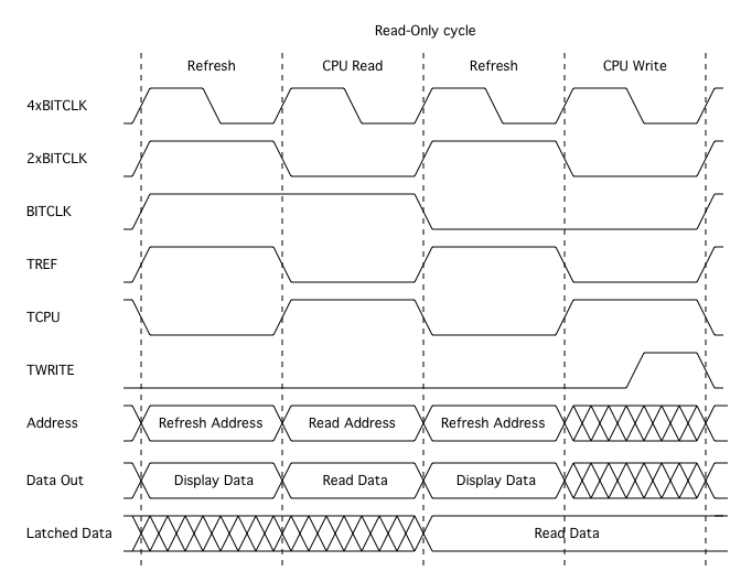
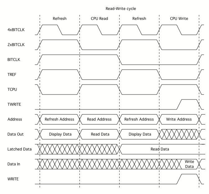
The plan is to divide each BITCLK cycle into four phases, of which two are refresh/display cycles, one is a CPU read cycle and one is a CPU write cycle. The following timing diagrams show what happens during one BITCLK period when the CPU performs a read-only cycle and a read-modify-write cycle.
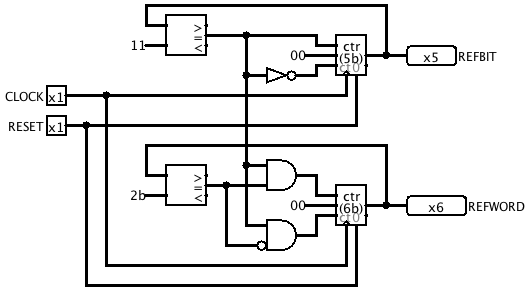
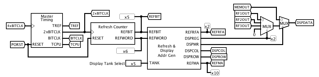
 The required timing and address signals are generated by the Master Timing and Refresh Counter circuits. They contain a bit counter that counts from 0 to 17 and a word counter that counts from 0 to 43. The first 32 word counts address the main memory to refresh it and generate data for the display. The next 12 word counts are used to read display data from the register file.
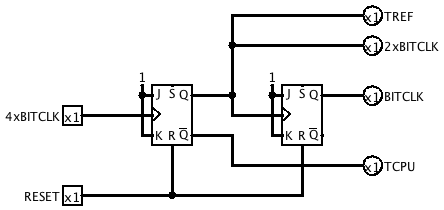
Master Timing:
 Refresh Counter:
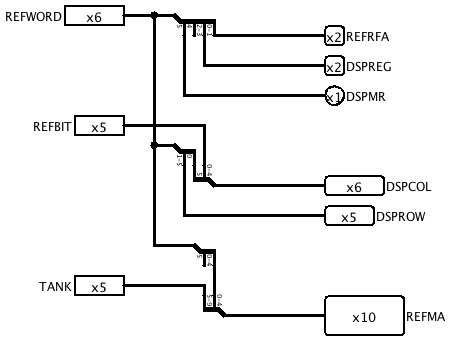
 The bit and word numbers from the refresh counter are rearranged and combined with a user-selected "tank" (memory page) number to produce addresses for the main memory and register files and control signals for the display. REFMA is the refresh address for the main memory. DSPREG selects one of the three register files and REFRFA selects a word from that file. DSPMR chooses whether to display data from the memory or the registers. DSPROW and DSPCOL indicate the row and column of the display for which data is being sent.
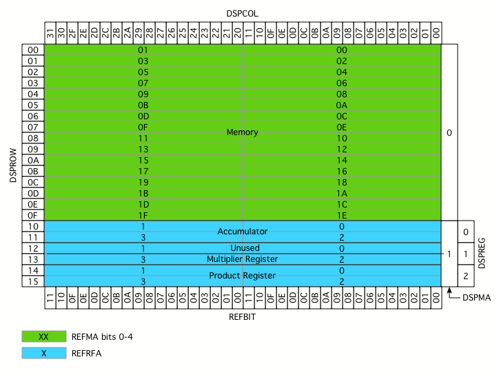
 The purpose of this particular arrangement is to generate a display laid out as illustrated below.
 These subcircuits are connected on the main circut as follows.
 Multiplexers have been inserted into the memory and register file address lines to switch been refresh and CPU addresses, and some other minor changes made to ensure that things happen in the right phases of the BITCLK cycle.
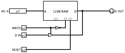
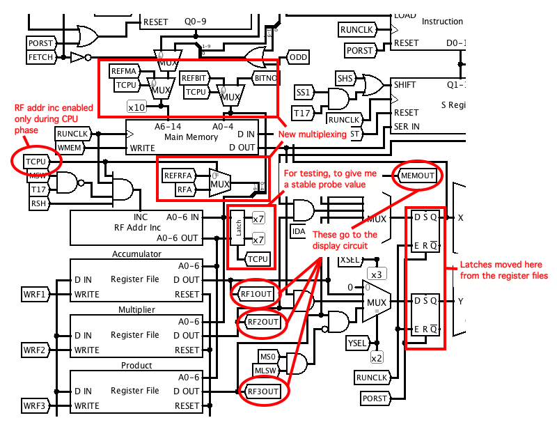 I moved the latches on the outputs of the register files out of the register file subcircuit and put them before the X and Y ALU inputs, because I need the raw outputs from the registers to send to the display. Also, I realised that I don't need to gate the write input to the static RAMs with RUNCLK, because this is already done when generating TWRITE. The register file simulation subcircuit is now just:
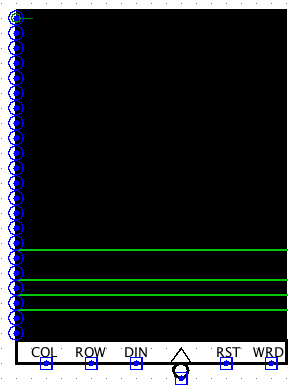
Testing the display circuit in Logisim
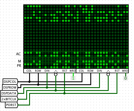
In the actual machine, DSPROW and DSPCOL will be used to generate X and Y scanning voltages for the oscilloscope, but Logisim doesn't simulate analog circuitry, so I put together a digital display using an LED Matrix component for testing purposes. I built a driver subcircuit consisting of 22 row drivers, each of which contains 18 individually addressable one-bit registers.
Row driver:
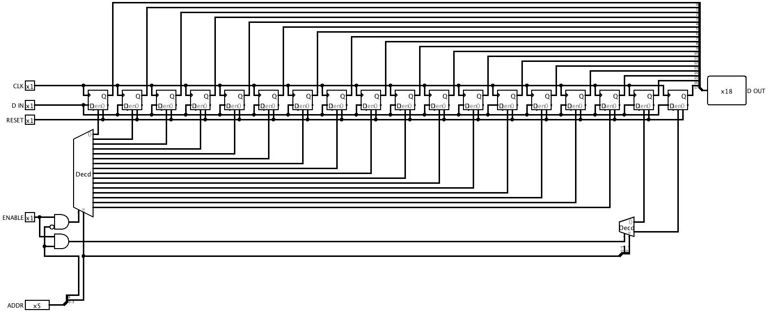 I made the circuit symbol for the row driver one grid unit high, so that I could stack them up next to a decoder in the matrix driver (although this turned out not to help much, since I couldn't find a compact way to arrange the outputs).
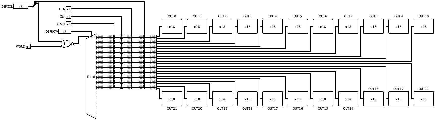 I designed the circuit symbol for the matrix driver to sit behind the LED matrix and provide a backdrop for it, as well as allowing two 18-wide matrices to be positioned side by side to form a 36 bit wide display.
 It took a bit of fiddling to get this to work properly, because the order in which Logisim draws overlapping components on a schematic seems to vary randomly depending on exactly how things are positioned, and to make things worse, it changes every time the circuit is reloaded from a file. But when the planets are aligned, it looks pretty good.
Discussions
Become a Hackaday.io Member
Create an account to leave a comment. Already have an account? Log In.