 Dylan Brophy
------- AWESOME CIRCUIT SIMULATOR -------
Use the above website to import and simulate the txt files I uploaded to this project.
The circuit simulator is really fun, I spend literally hours on it. Check out the designs I came up with!
Random stuff I do with TTL, CMOS, and transistors. probably lots of programmable logic.
Already have an account? Log in.
To make the experience fit your profile, pick a username and tell us what interests you.
------- AWESOME CIRCUIT SIMULATOR -------
Use the above website to import and simulate the txt files I uploaded to this project.
The circuit simulator is really fun, I spend literally hours on it. Check out the designs I came up with!
DTTL LUT.txtA lookup table made with transistors.plain - 2.59 kB - 07/01/2018 at 04:13 |
|
|
DTTL inverters.txtusing both an NPN and PNP transistor for logic outputplain - 2.26 kB - 07/01/2018 at 04:13 |
|
|
DTTL double LUT clock.txtTwo LUTS configured as one inverter and one buffer, connected to produce a clock signal.plain - 6.35 kB - 07/01/2018 at 04:13 |
|
|
DTTL NAND.txtNAND gate with both NPN and PNP transistors for logic outputplain - 1.61 kB - 07/01/2018 at 04:13 |
|
|
DML logic family.txtdiode-MOSFET-logic family (insted of DTL)plain - 2.02 kB - 07/01/2018 at 04:13 |
|
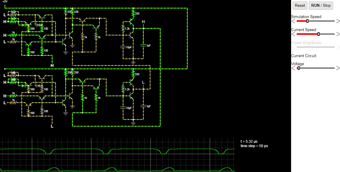
Normal voltage requirement is 2v, switches at about 600mV. All transistor betas are 100.
The capacitors are for simularing parasitic capacitance.
The above circuit is two LUTs connected to make a clock. One is configured as a buffer, the other as an inverter. The 8 inputs on the left tell the LUT what values are where. The inputs on the bottom of the LUTs are the address. The image above is at two volts input power.
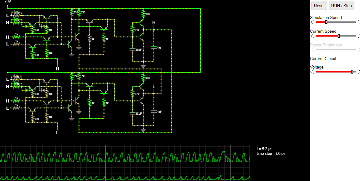
The circuit can take voltages up to about 11v before the logic stops working. This is at 11V to see how it switches right before the voltage that it stops working (between 11v and 11.16v). there is a lot of ringing for some reason, probably due to the small capacitors to simulate parasitic capacitance.
I felt like building an FPGA slice, so I did.
Based somewhat upon Nick's Blog entry here.
Sorry for the bad photo, my phone has issues.
Essentially the bottom three ICs are 74hc595 (CMOS logic levels) for allowing an arduino to program the slice. The three ICs up top are two 8:1 MUXs and two D flip flops. The oscillator up top is connected to the D flip flops, so they always have updated values.
I used CMOS chips because I did not have enough TTL MUXs, even though I have plenty of every other TTL IC...
I may consider making many FPGA slices and connecting them together one day, with printed PCBs and such. Those would have DIP switches instead of 74595s because DIP switches are more fun to program.


Indeed. I haven't had as much time since I graduated HS and got a job, but I now do engineering work professionally so I don't mind. I feel like I will come back to it someday, when I need a break from my work to do something more lighthearted XD

the circuit simulator is amazing!!!
thank you so much for putting all of these schematics together!
awesome!!
No problem! I am glad someone found them and enjoys them so fast. I will be sure to post more sometime.
Which circuit is your favorite?

 will.stevens
 alexboes17
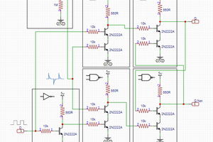

 Blair Vidakovich
Sadly there is no recent update.