0%
0%
Z80 Single-board computer (with AVR controller)
Another Z80 single-board computer.
 Scott
ScottBecome a Hackaday.io member
Already have an account? Log in.
Just one more thing
To make the experience fit your profile, pick a username and tell us what interests you.
Pick an awesome username
hackaday.io/
Your profile's URL: hackaday.io/username. Max 25 alphanumeric characters.
Pick a few interests
Projects that share your interests
People that share your interests

 Keith
Keith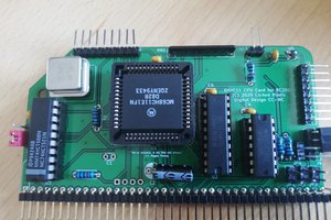
 EtchedPixels
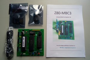
 eprive
 Plasmode
Saturday, October 8, 2016
Working on the SPLD to use as an I/O decoder. I have GAL20V8Z's available and the free WinCUPL from ATMEL. I needed five chip selects; UART, PIO, DISK, RAM1 and RAM2. I would like to implement a wait-state generator in case I need to use it at the higher Z80 clock speeds. My first stab at it was a simple I/O decoder splitting the ROM up to access at 0x0000 to 0x00FF and 0xE000 to 0xFFFF, RAM1 at 0x0100 to 0x7FFF and RAM2 at 0x8000 to 0xDEFF. I needed to use A[15..8] along with the MREQ and IORQ lines. Oops! WinCUPL failed because I needed too many product terms. I then tried the same with a GAL22V10 and it fit, so I ordered some but they are 3 to 4 weeks away coming from China. Next I committed myself to nix the ROM, which allowed me to use just A[15..12], thereby simplifying my design to fit into the GAL20V8Z's I have. I really wanted to test my code in a live Z80 environment so I wired up a solderless bread-board with a simple ATmega328P, a Z80 with all data lines held low (to execute NOP's) and the GAL20V8Z. The AVR conrols the RESET and CLOCK lines so I wrote a quick program to initialize them and drive the Z80. The photo of the solderless bread-board used for testing this phase of the design is attached.
Note on the GAL20V8Z; it has a nive power-saving feature wherein it looks at all the input pins. If all of them do not change state for a certain time period, the part goes into a low-power standby mode util it sees activity again. Since I am using it as an I/O decoder, I don't see that it will ever get to switch into power-saving mode.
I had some problems getting the GAL20V8Z to function properly. The UART select kept toggling with the MREQ line. Wierd since the simulation showed all test vectors with correct results! After many hours of re-coding CUPL and re-burning GAL20V8Z's, I started to get the impression that it was the programmer because even the simplest boolean equations burned in the SPLD did not function correctly. Since the programmer would let me select GAL20V8, GAL20V8A ,GAL20V8B, GAL20V8C and GAL20V8D parts, tried the GAL20V8D device and it started to work, I was using the GAL20V8 setting, which turned out to be the culprit. Odd since all five parts have the same number of bits in their fuse map.
After getting the I/O decoding to work, I set out to design in the wait-state generator since I had a few output pins left on the GAL20V8Z. I used the 74xx74 D-flip-flop reference right out of the Z80 data sheet. The simulation worked correctly, hi-z until it drove the Z80 WAIT pin low. In reality, I could not get it to work as the WAIT pin never went low. Grounding the OE pin (13) on the GAL20V8Z allowed me to see the states of the internal "wait 1" and "wait 2" signals from the registers and I found the problem, which was corrected. So after several hours diddling with the wait-state generator, I had it working at the 8MHz Z80 clock speed. Time to try lower clock speeds. After switching gears to 4MHz, I could see that the Z80 was held in a perpetual WAIT cycle. Switching back to 8MHz and the problem cleared. Hmm... This should not be happening as the internal flip-flops are clocked by the Z80 clock and driven by the MREQ line. A few more hours of diddling and I decided that if I was going to need the wait-states, they would be at the 8MHz clock speed so I added a WS-EN (wait-state enable) pin to be driven by the AVR. If the AVR is generating 8MHz for the Z80 then it will enable the wait-states, if not, then it disables the wait-state generator and now the Z80 functions fine at the lower clock speeds, all the way down to 31.250KHz. After musing over the RAM IC data sheets for the IDT and CYPRESS 32Kx8 static RAMS I have, the cycle time is 150ns between sequential reads. It is likely that I will never need wait-states for the RAM ... but I may need them to interface with the AVR UART and DISK emulation.
Next up; Interfacing with the 74HC299.
If anyone has any input on why the wait-state generator only functions when the clock speed is 8MHz, I have posted the CUPL code below and I would appreciate some feedback and/or tips.
[code]
Name Z80_IOdecode-1V10;
Partno Z80C;
Revision 01;
Date 9/20/2016;
Designer Quest, Johnny;
Company KSV;
Assembly Z80 Computer;
Location U4;
Device g20v8a;
/*******************************************************
* ___________
* | Z80_IOdec |
* sys_clk x---|1 24|---x Vcc
* !mreq x---|2 23|---x !rst
* !iorq x---|3 22|---x UART_sel
* ws_en x---|4 21|---x PIO_sel
* x---|5 20|---x !DSK_sel
* x---|6 19|---x wait1
* x---|7 18|---x wait2
* a12 x---|8 17|---x !WAIT
* a13 x---|9 16|---x !RAM1_sel
* a14 x---|10 15|---x !RAM2_sel
* a15 x---|11 14|---x !m1
* GND x---|12 13|---x !oe
* |____________|
*/
/*******************************************************/
/* This device generates chip select signals for two */
/* 32Kx8 static RAMs. */
/* It also drives the system WAIT line to insert a */
/* wait-state of at least one cpu clock for all memory */
/* accesses. 1 wait-state is internally generated by */
/* the Z80 for I/O accesses */
/*******************************************************/
/** Inputs **/
PIN 1 = sys_clk; /* System Clock */
PIN 2 = mreq; /* Z80 MREQ (active low) */
PIN 3 = iorq; /* Z80 IORQ (active low) */
PIN 4 = ws_en; /* Wait-state enable (active high) */
PIN [8..11] = [a12..a15]; /* upper 4 address bits */
PIN 13 = !oe; /* Output Enable (active low) */
PIN 14 = m1; /* Z80 M1 (active low) */
PIN 23 = rst; /* System reset (active low) */
/** Outputs **/
PIN 22 = UART_sel; /* 82C51A UART (active high) */
PIN 21 = PIO_sel; /* 82C55A PIO (active high) */
PIN 20 = DSK_sel; /* SDmemory interface (active low) */
PIN 19 = wait1; /* Internal Use (combinatorial logic out only) */
PIN 18 = wait2; /* Internal Use (combinatorial logic out only) */
PIN 17 = WAIT; /* insert 1 WAIT-STATE (active low) */
PIN 16 = RAM1_sel; /* 32Kx8 RAM (active low) */
PIN 15 = RAM2_sel; /* 32Kx8 RAM (active low) */
/** Declarations and Intermediate Variable Definitions **/
FIELD address = [a15..12]; /* upper 4 addresses */
uart_eqn = !iorq & !m1 & address:[0000]; /*******************************/
pio_eqn = !iorq & !m1 & address:[1000]; /* */
dsk_eqn = !iorq & !m1 & address:[2000]; /* I/O Address */
/* Ranges */
ram1_eqn = !mreq & !m1 & address:[0XXX..7XXX]; /* */
ram2_eqn = !mreq & !m1 & address:[8XXX..FXXX]; /*******************************/
/** Logic Equations **/
/* UART/PIO select (active high) */
UART_sel = uart_eqn; /* high for addresses 0000h-0FFFh */
PIO_sel = pio_eqn; /* high for addresses 1000h-1FFFh */
/* DSK select (active low) */
DSK_sel = !dsk_eqn; /* low for addresses 2000h-2FFFh */
/* RAM select (active low) */
RAM1_sel = !ram1_eqn; /* low for RAM addresses 0100h-7FFFh */
RAM2_sel = !ram2_eqn; /* low for RAM addresses 8000h-DFFFh */
/* wait state generator */
wait1.d = (!mreq # !iorq); /* Synchronous Wait-state */
wait2.d = wait1; /* wait1 delayed */
WAIT.oe = ws_en & wait1 & !wait2; /* Turn Buffer ON */
WAIT = !(ws_en & wait1 & !wait2); /* End Wait */
[/code]