Close
0%
0%

TS350 True Sine Inverter

350 Watt inverter that converts 12VDC to 120VAC @ 60Hz.

Similar projects worth following
This project is the next iteration of the TS50 to design & build a practical, light weight, true sine inverter.

I first mentioned the TS350 in the TS50 project and that it represented the culmination of prior R&D.  I had expected that it would probably go thru a few iterations to work out all the bugs but that on the whole it would be a working design.  I had to rethink my definition of ‘working’.  I’ve been at it now for two months and have a path forward for a redesign so,I figured this was a good time to start the project write-up.  For background & context read about the TS50 first.

I designed the TS350 as an inverter capable of sourcing 350W continuous with the ability to deliver 500W (limited by operating temperature) for short durations.  It was to do this over a wide input voltage range of 11 - 30 VDC so it could work with 12-28V systems.  Not a problem, the inverter section would employ a traditional control loop to maintain a regulated 170VDC to the sine section.  To do this with a full bridge and maintain flux balance in the transformer core requires a center-tap, full wave rectifier configuration.  The inductor in the output LC filter maintains current flow thru the transformer secondary during the bridge off time which prevents the core from resetting.  I had validated all of this in the TS50 platform.

Or so I thought.  I had built center-tap transformers in the TS50 but their secondaries only delivered 60V.  The TS50’s transformer delivers 170V but it is not center tapped.  This turned out to be my big miss.

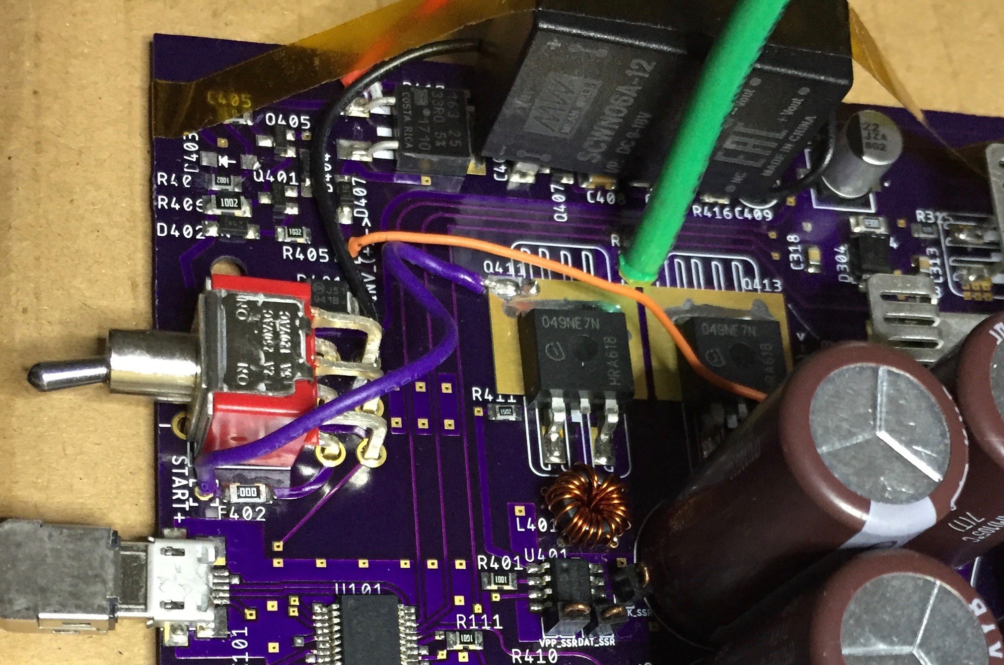
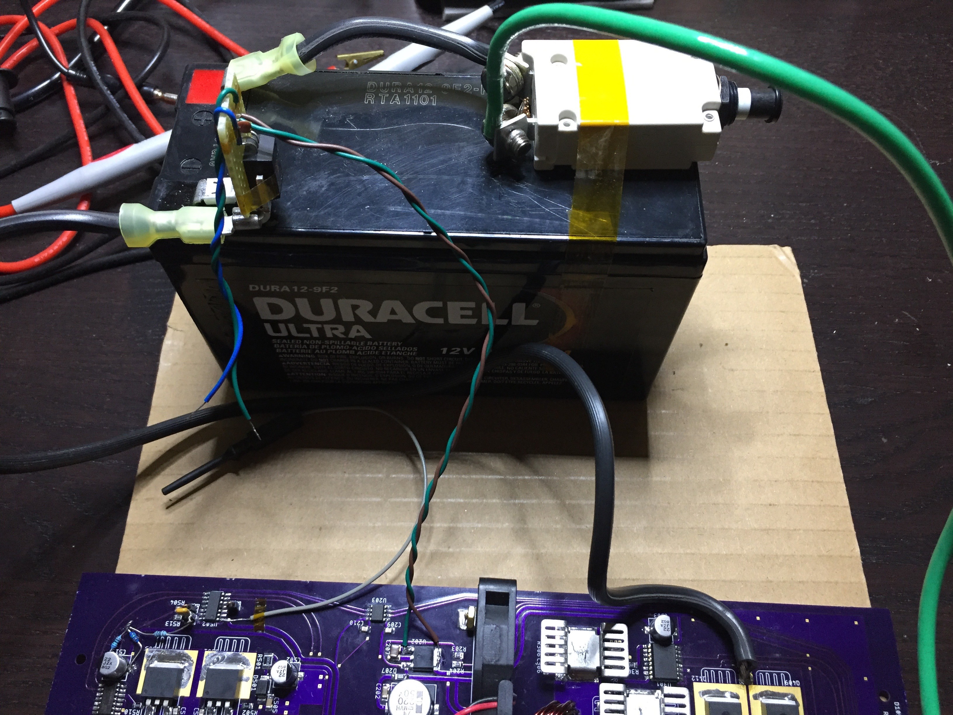
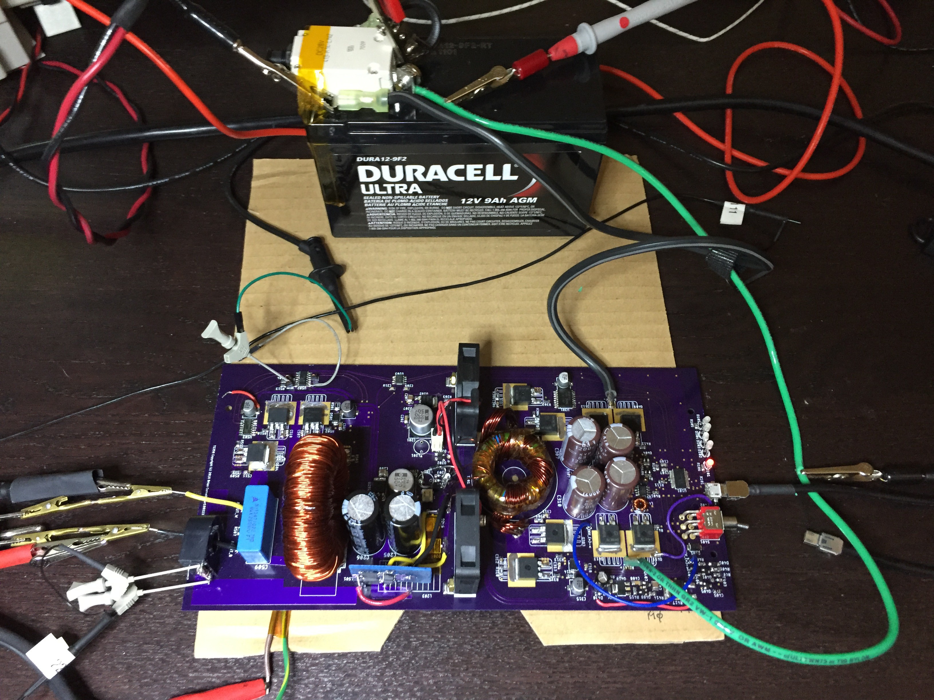
So I get my shinny PCB from the fab and start assembling section by section, testing as I go to:  controller - check, start circuit - mostly check, bridge - check.  I install the toroid wound transformer to test before moving on to the secondary supplies & sine section - don’t want it destroying things.  I fire it up and take a look at the outputs:  it shows a very large resonant ring but is otherwise functioning as expected.  I’ve seen this before and many SMPS transformers will do this with their secondaries open so I’m not overly concerned.  I complete the secondary power supplies, hook-up the DC load, and that’s when the trouble begins.

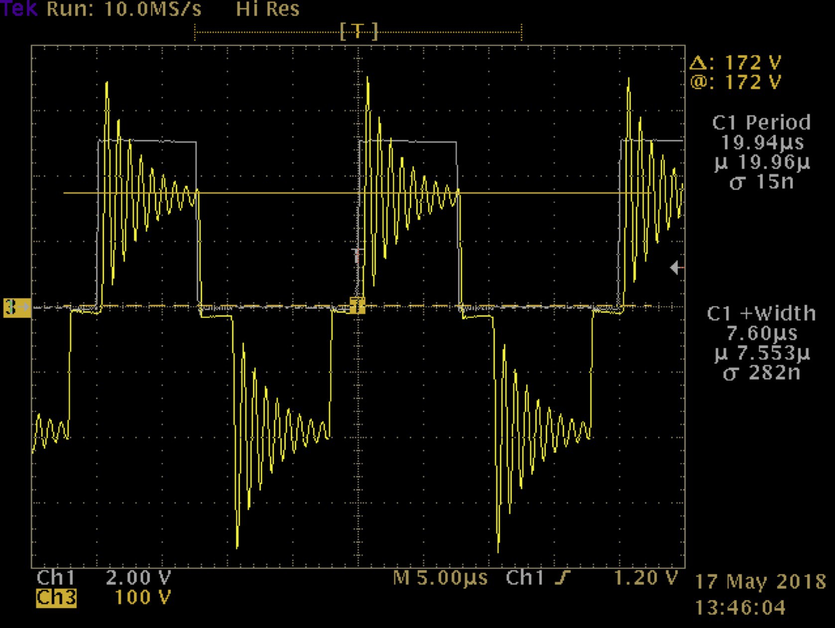
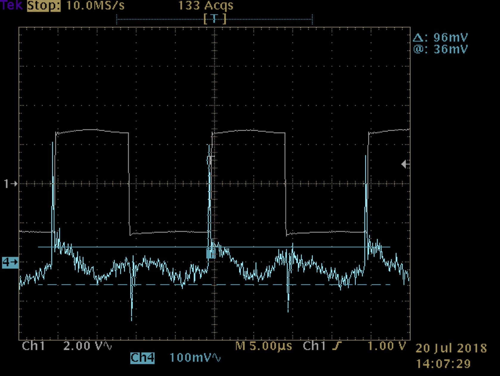
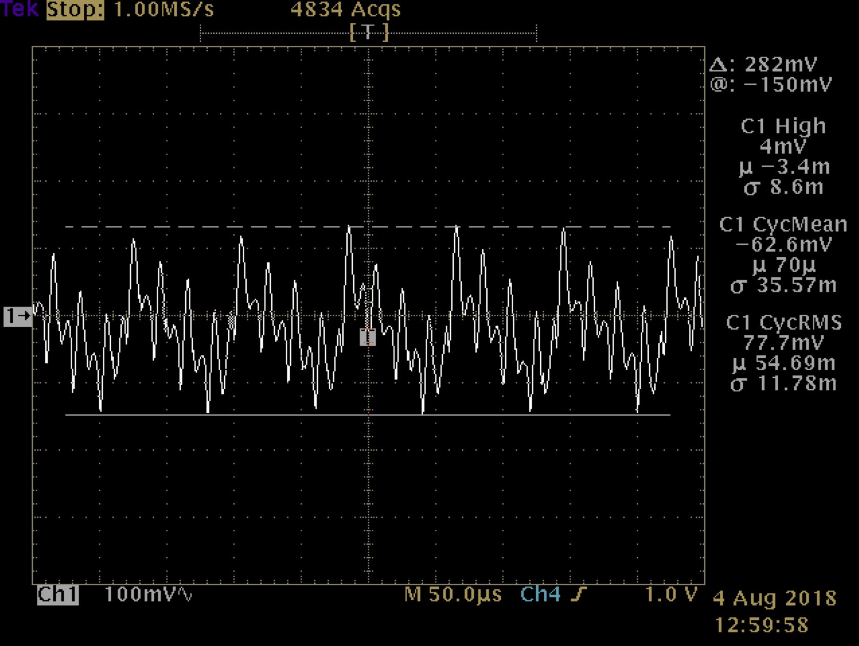
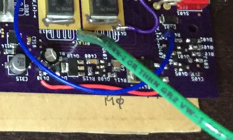
Above is the waveform at the anode of one of the rectifiers with a 1A load applied.  Note the scale for CH3 - 100V.  The cursor marks the 'no ring' expected voltage.  The amplitude of the first ring cycle is nearly 200V!  Even with 35nS reverse recovery times and generous thermal pads the rectifiers run hot (>50C) due to the ring.  High loads make it worse.  Higher input voltages make it worse.  Of course this ring is reflected to all the windings.  It renders my primary current sense circuit useless.  It’s amazing the thing runs at all.  After mucking with it for a few hours it’s obvious that a transformer rebuild is required or the design is DOA.

So started a two-month journey to come up with a working transformer.  Along the way I earned another degree from the school of hard knocks:  when designing a power supply - any kind - always start with the transformer.  I had done this but with an inadequate working knowledge of high voltage windings.

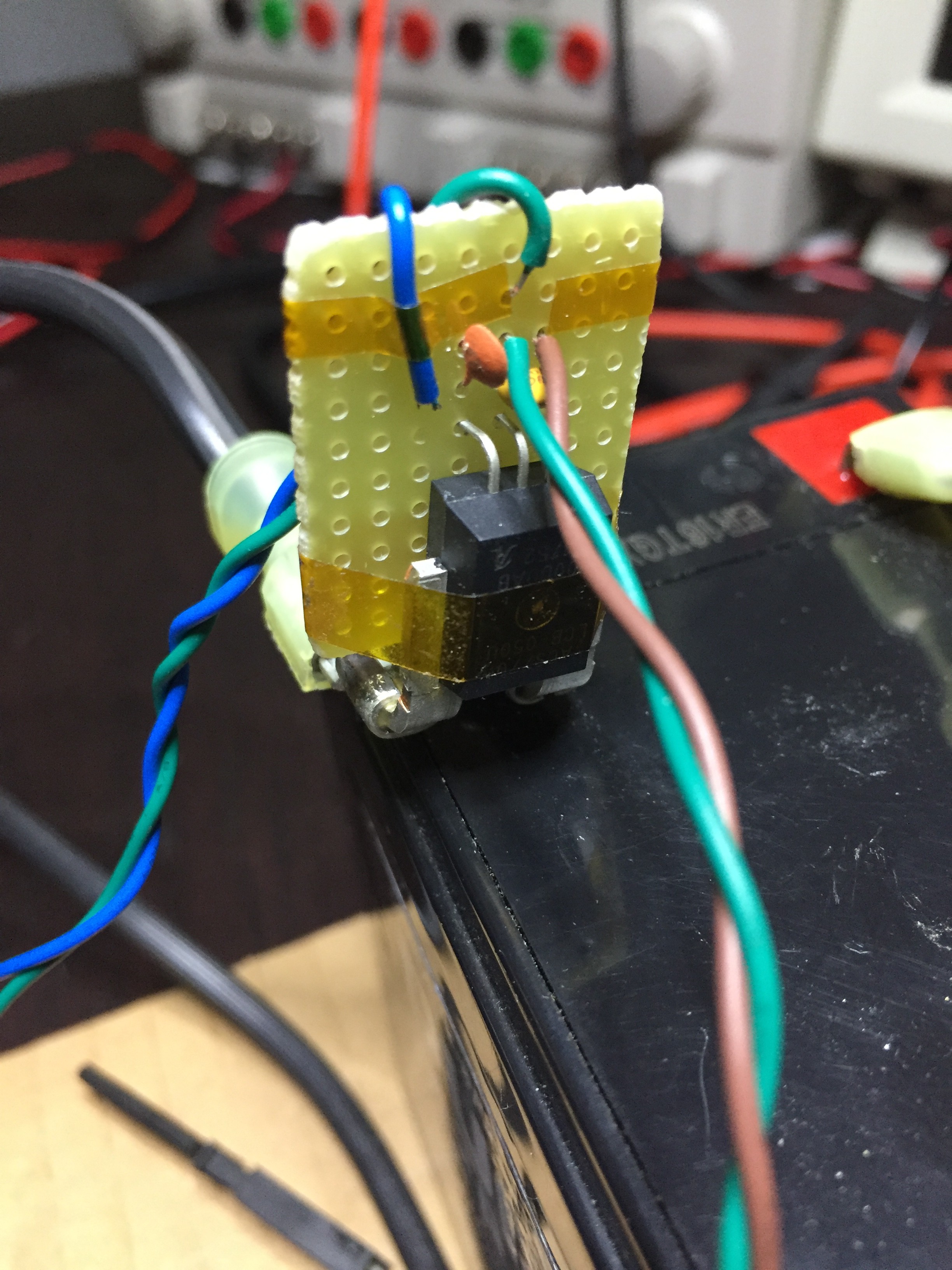
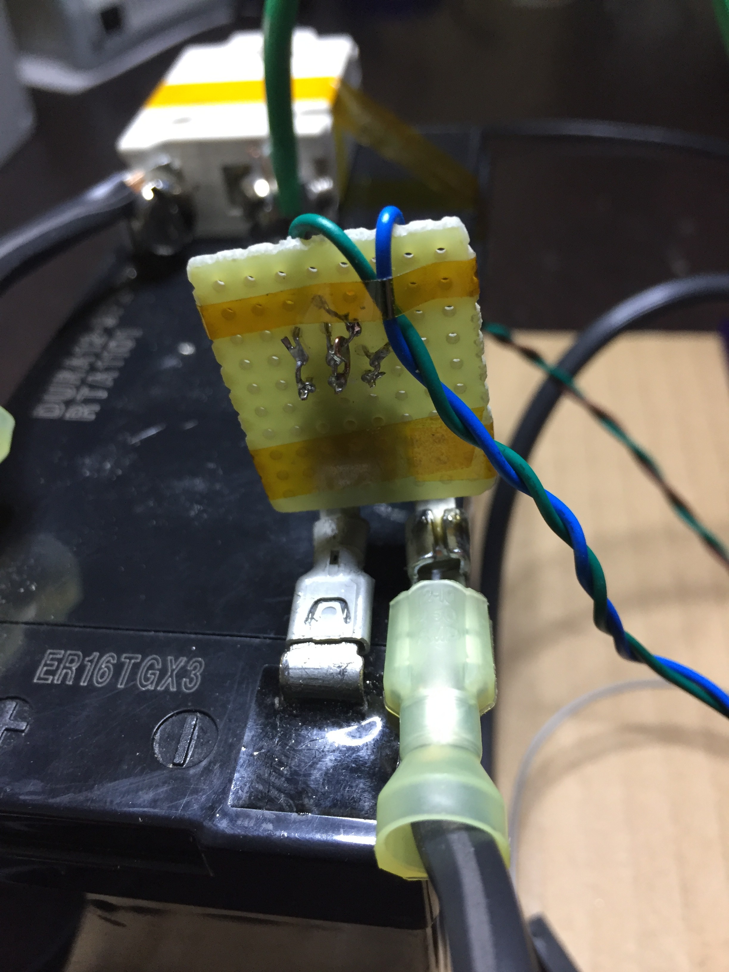
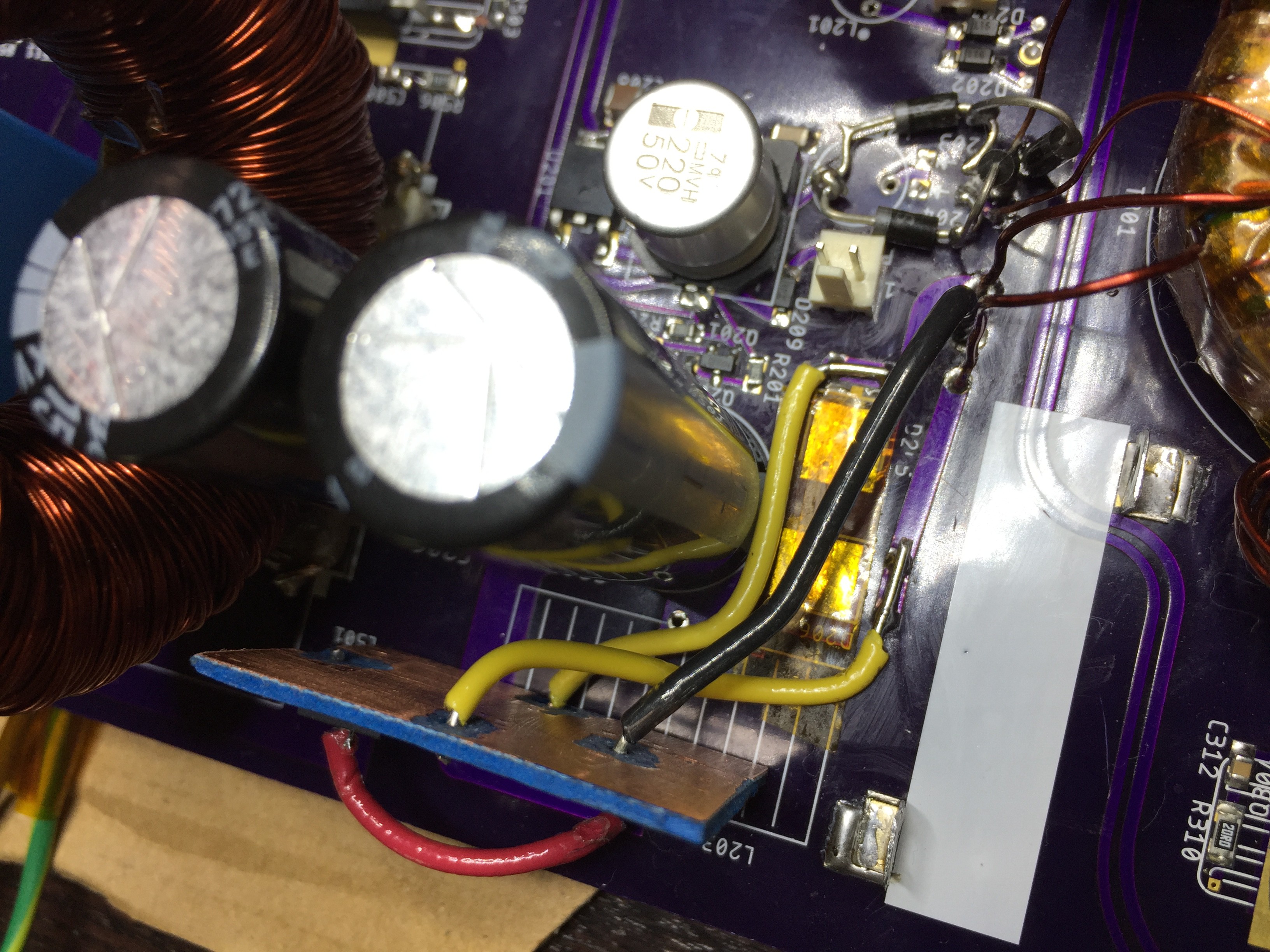
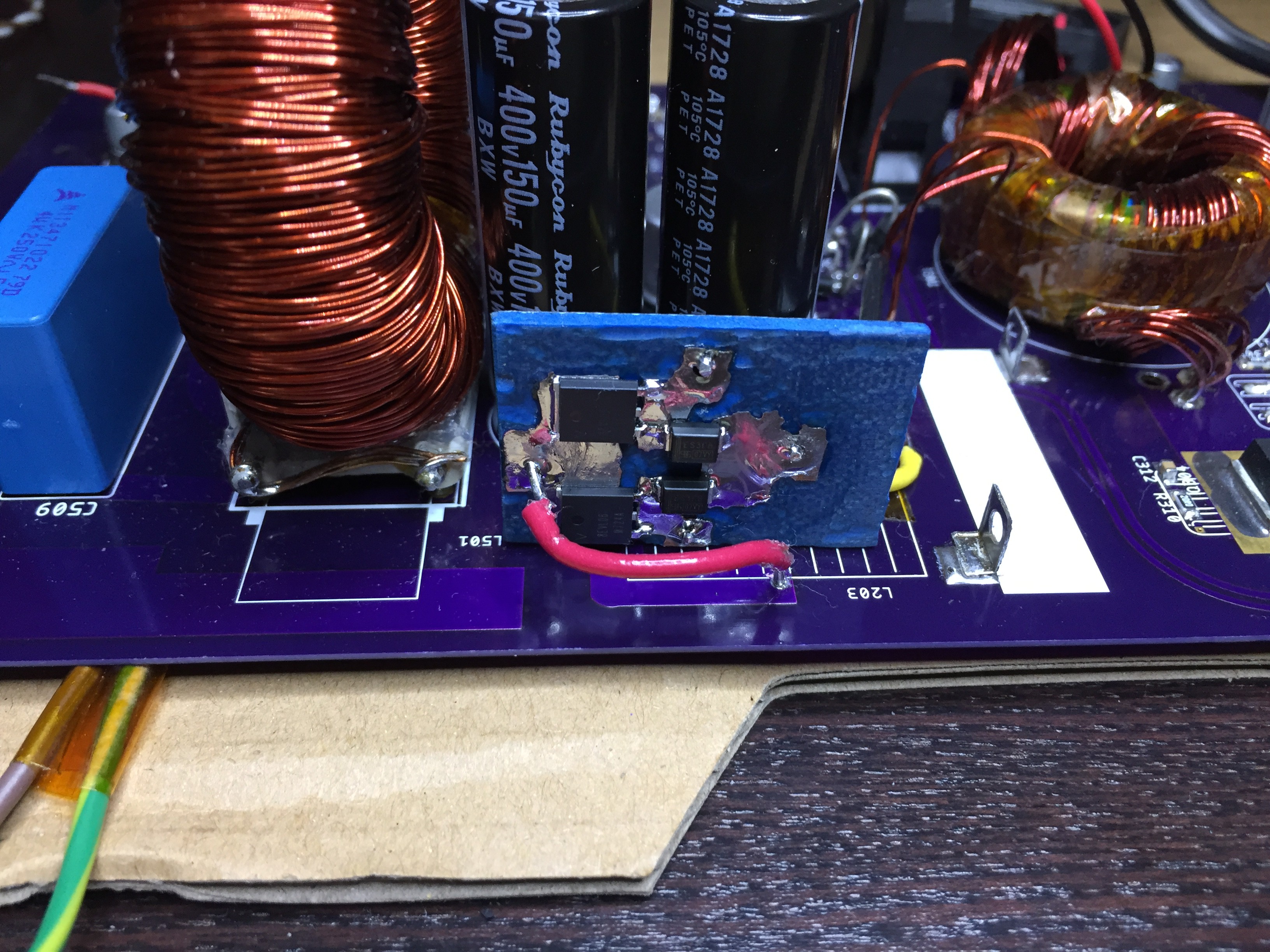
I built-up another copy of the full bridge board used in the TS50 (easy to swap transformers) and proceeded to test a dozen different builds using RM & toroid cores with a variety of winding configurations.  Interleaved, bifilar, interleaved & bifilar, foldback, single layer, a combination of all of them.  Faraday screens too:  for both primary & secondary.  But it didn’t matter - the results were consistently bad.  The ‘best’ design had a measured lumped parasitic capacitance of 10nF and the worst greater than 130nF but in-circuit their performance was almost indistinguishable:  a resonant ring with a peak amplitude greater than 100V above the design voltage with a decay lasting the entire duty cycle (5-90%).  

The frequency of the ring...

Read more »

ts350-180223-a0-bom.xlsx

TS350 BOM for original design.

sheet - 27.54 kB - 07/10/2018 at 16:44

Download

ts350-ctrl-1_0_b51.X.zip

TS350 original design for MPLab project source for main controller including debug & hack code used during redesign.

Zip Archive - 755.64 kB - 07/10/2018 at 15:40

Download

ts350-sine_48-1_0_b9.X.X.zip

TS350 sine controller MPLab project source used in original design and redesign work. Includes compile options for fixed & voltage dependent tables.

Zip Archive - 276.20 kB - 07/10/2018 at 15:40

Download

ssr-12f1612-2-1_b7.X.X.zip

TS350 relay controller MPLab project source used in original design.

Zip Archive - 215.64 kB - 07/10/2018 at 15:40

Download

ts350-180223-a0.zip

TS350 Eagle PCB files for original design.

Zip Archive - 223.87 kB - 07/10/2018 at 15:34

Download

  • Moving on

    Brian Cornell03/30/2019 at 18:52 0 comments

    This project has served me well and I've probably taken it as far as it can go in it's current form.  I've hacked it countless times modifying the firmware, testing thermal management, different output filter configurations, etc.

    I'm hoping it's work will live on in a redesign.  Boards are at the fab and once assembled I'll start posting under a new project.

  • Thermal Evaluation

    Brian Cornell12/01/2018 at 20:03 0 comments

    After some diversions on other work I'm finally getting around to working on the TS350's redesign again.  I did a poor job on the original thermal model and didn't account for the increase in Rds(on) of the MOSFETs (with temperature) and, more importantly, the coupling of adjacent components.  The result was that the inverter section would overheat (shutdown) at continuous operation much above a 300W output.

    One of my enlightenments after some additional book work is the need for thermal imaging to get a true picture of what's going on; my spot IR thermometer & thermocouples don't cut it.  I picked up a FLIR One Pro.  Because it uses a smartphone for display & processing it's half the cost of an entry level professional, self-contained, IR camera.

    It's easy to use and with the companion FLIR Tools application enables you to quickly analyze image data.  Here's an image of the TS350 powering a 300W load continuous.  The temperature boxes were added after the image was taken with the Tools appl.

    The camera paid for itself on the first use.  Revelations:

    • Box 1:  the high-side sine switches run much hotter than the low-side, even though they are on only half-time (vs. the low side on ~ 85% of full sine cycle).  Why?  Because the high side experience high voltage & current switching stress (at turn on there is a +170V gradient D-S) whereas the low side switches under near 0V conditions.  A secondary contributor is the higher thermal coupling coefficient of the high-side transistors since adjacent to one another.  Duh.
    • Boxes 2 & 3:  my model over-estimated the temperature rise of the relay MOSFETs.  I didn't install heat sinks and they are running close to my model's predicted temperatures with heat sinks.  Also note that the temperatures between the +/- poles are symmetrical (good).
    • Box 4:  thermally speaking the inverter MOSFETs are my problem child but at first glance the image doesn't reflect that.  The hot spot in the box are the current sense resistors and, while not a surprise, is a reminder to be careful with their location and coupling effects to & from them.  Heat sinks are installed on the switches and they are quite cool.  But most of the board area around them is copper and the image shows those temps >70C.  My conclusion is that the heat sinks do a poor job of conducting heat from the board and that leads to high case / junction temperatures.  As with the sine MOSFETs, the coupling effect doesn't help.

    My take-away is that SMD heat-sinks are okay when dealing with only a few watts for a single device but for higher powers & multiple devices they are inadequate.  I suspect they can also present a significant near-field capacitive coupling problem with few remediation options other than a shielded enclosure.

    So, for the redesign I am creating a linear superposition model that will account for coupling effects.  To do this requires that I know the coupling coefficients and these must be measured from a thermally representative model of the design.  All of this implies that I need to make decisions on the board layout, transistor mounting, heat sinks, etc.

    I'm definitely gong with TO220 MOSFETs for the inverter with the goal of a more compact footprint and improved thermal efficiency.  The relay will remain SMD but will probably offload to a separate power board that contains the power connections, user interface, etc., and because of this probably won't need heat sinking.  I haven't decided on the sine section yet.  From an EMI perspective it needs lots of improvement and much of it will revolve around reducing the size of current loops.

    Lots to do!

  • Current Monitoring and Control

    Brian Cornell10/19/2018 at 19:43 0 comments

    Objective.  A design goal for TS350 was to leverage a single current sense circuit that could provide both pulse-pulse, or Safe Operating Area (SOA), protection and average / RMS current for power management.  Cost and space were key drivers.  I prefer to use current transformers because of their inherent low noise, galvanic isolation, and undistorted output, but in this design they don’t support the objectives.  First, they are relatively large.  More importantly, using a single CT for both sides of the bridge with a high fixed duty cycle won’t provide sufficient time to reset the core without flyback voltages in excess of 200V.  To avoid this I’d need to use two and that would require additional downstream circuitry.

    Current Sense Design.  A high-side sense resistor and differential amplifier are used for current sensing.  Compact and cheap.  The trade-off is a not so clean signal that requires downstream conditioning.  I opted for high side sensing to avoid / reduce the incidence of problems associated with COM below ground for the gate driver.

    Reference the schematics posted to the project to follow this description.  R307 & R308 are paralleled to form the sense resistor.  Their paralleled value of 1.5mΩ produces a differential voltage of 1.5mV/A.  U302 is a TI OPA197 rail-rail, high speed Op Amp.  R316 sets 10x gain for an output of 15mV/A and, Q305 level shifts (removes the INV_(+) supply voltage) the output for direct processing by the MCU, U101.  R311 & R312 provide current limiting and in conjunction with D302 & D303 protect the Op Amp from voltage spikes.  C314 & C317 provide local bulk capacitance and decoupling.  Note that the supply voltage for the Op Amp is the direct input voltage and not the inverter auxiliary supply (VCC_INV).  This is necessary for it to function - it’s inputs can’t be at higher voltages than its supply.  This will be true for the redesign as well.

    SOA Protection.  The image below depicts the MCU’s peripheral configuration that performs both SOA and current averaging.  Comparator CM2 is responsible for SOA protection.  It’s positive input is connected to voltage reference DAC1 to define the over-current limit (in the prototype the limit is set to 140A).  The negative input is connected to the external current sense circuit’s output.  Ideally CM2’s output would connect directly to COG1 to drive a Falling Event (FE) input to terminate the drive pulse but it was previously mentioned that signal conditioning is required.

    In this figure channel one is the output of the current sense circuit with a peak current of 48A.  The ideal waveform would be the ‘ramp on a step’ (trapezoid) with no +/- spikes.  The curved leading edge is due to the rise time of the Op Amp.  Some of the positive spike at pulse termination is due to probe parasitics (as is the ring at pulse start) but much of the negative spike at pulse start is real.  This created problems that the COG’s native blanking feature couldn’t handle (the MCU would reset).  The redesign will incorporate a protection diode across the sense input to ground but even that may not be sufficient given the pulse amplitude.

    A more flexible blanking circuit was fashioned using MCU peripherals CLC3 and PWM11.  The PWM is slaved to the master, PWM5, and set to the same frequency.  PWM11’s duty cycle defines the blanking time.  CLC3 will only allow a FE outside of the blanking time.  It is possible for a FE to occur at the end of the DC but that is non-consequential since the master PWM has already terminated the pulse with a FE.

    The firmware protects the inverter from continuous over-current events.  When running, COG1’s duty cycle is sampled on each pass of the run loop.  A simple PID filter sets the limit on time & rate (integration is somewhat variable based on loop timing) of over-current...

    Read more »

  • Auxillary Power Supplies

    Brian Cornell10/14/2018 at 20:43 0 comments

    The hacks made to the prototype allowed it to function for testing but the fans limited the input voltage range to less than 14 volts.  I wanted a simple & efficient method for regulating the inverter's auxiliary supply.  The sine section would need this too.

    Since the redesign settled on the inverter operating as a DC transformer the option of a control loop was out.  The discrete LDO I used in the start circuit wasn't suitable for delivering 300+mA so I began to look for off-the-shelf solutions.  I looked at linear LDOs but their dissipation was too high.  Their temperature derating was also a problem.  I considered building my own buck/boost - more time consuming than I wanted.  I eventually settled on a 6W isolated monolithic switching supply from Mean Well.  It has current limiting, short circuit protection, decent transient response, acceptable noise margin, and provides a stable 12V from 9 to 18 volts.

    I purchased one for evaluation and characterized it with an electronic load.  It performed to spec well with only one anomaly.  When running under greater than half load and applying a short, the unit would not restart with the short removed.  I wound up contacting the OEM and confirmed it was working as designed.  I was a bit surprised to hear that since when testing my own designs I consider that a conditional stability problem.  But, this unit was nearly half the cost of the competitor's unit and I didn't anticipate loads or transient conditions that would make this a problem even when considering temperature derating (incidentally, I did test the other unit and it didn't have the problem).

    I decided to use the Mean Well and added to the prototype.

    Without fans to power, the sine section would have very modest power requirements (100mA max).  A switching regulator would be a waste in both cost & space.  A linear LDO regulator like the MC7812 is cheap, small, and wouldn't dissipate more than 1W.  To provide isolation the redesign will use an auxiliary transformer winding with one additional turn than the primary.  This ensures that even at low input voltages the LDO will have several volts of margin to provide a stable 12V.

    I didn't make this modification to the prototype since it is basically using this design; the only change is to an LDO that can handle higher input voltages.

  • Differential Input Filter

    Brian Cornell08/15/2018 at 02:54 0 comments

    I didn’t include one in the original design but with the current setup I now have the ability to quantify the EMI footprint.  Spoiler alert:  I’ve concluded one isn’t needed.  Here’s why.

    With a 350W load the voltage ripple across the power source (a battery) is ~ 100mV P-P.  With a 400W output the current ripple is 3.56A P-P.  Why the discrepancy in loads?  These are the measurements I had on-hand and was too lazy to go back & redo.  Besides, they favor a worst case.  Here are the waveforms, voltage & current respectively.


    The required inductance for the filter can be calculated with the formula:  L=(Vr/Ir)TonToffT where Ton & Toff are time on & off in percent and T is the period in seconds.  Substituting:
            L = (0.1 / 3.56) x 0.95 x 0.05 x 1e-5
            L = 13nH

    Hardly worth it.  Note that this is with power leads measuring about 2 ft (66cm) each.  In a real-world application the power leads will likely be longer and even if they are paralleled or twisted will present a similar or larger inductance.  It also assumes a low impedance power source which is a necessity for this thing to operate correctly.  Using the above figures:  R = V/I = 12 / 3.56 = 28mΩ.  Assuming a 12V supply:  12 / 0.028 = 427A.  That’s probably a bit high for a 9Ah battery but even at half of that its impedance is only 56mΩ.

    While on the subject of input filters I’m not looking at common mode.  This board has a lot of EMI coming from the sine section with much of it due to poor layout.  Also the transformer doesn’t incorporate faraday screens so this will be left to evaluation in the revised build.

  • Getting Accurate Current Measurements

    Brian Cornell08/15/2018 at 02:15 0 comments

    With a functioning unit I can get on with using it to explore refinements for the next design iteration.  But a lot of that work requires being able to measure, with reasonable accuracy, the input current.  And therein lies the rub:  this thing can easily draw 40A RMS with peaks exceeding 50A.  I had mentioned in a previous post using the voltage drop across a measured segment of the positive supply lead but that is prone to noise and temperature error, particularly when using the scope.

    Bench equipment to do this is prohibitively expensive.  So are scope probes - most can't handle currents this high.  I could replicate a version of the sense resistor & opamp circuit in the TS350 but that is exactly what I am trying to calibrate (for average power measurements).

    Allegro hall effect current sensors to the rescue.  I've used these before and they're great for applications requiring accuracy but without a high dv/dt and they are very rugged.  I selected the 50A DC ACS770LCB-050U-PFF-T.  For about $10 and some elbow grease I have an accurate input current sense that will render a reasonable picture of the current ripple.  Response / rise times are on the order of ~ 6uS.

    Here's a picture of the setup:

    The sensor is fastened to perf board to facilitate power & output connections along with the decoupling and output filter caps.  The current sense leads (PFF leadform) are connected to female clam connectors for direct connection to the battery negative and return lead from the inverter.

    And here's the full setup:

    The sensor requires a 5V supply and this is taken directly from the unit's 5V LDO (green/brown pair).  Sensor output is the blue/green pair.

    A nice side-benefit of these sensors is galvanic isolation; not critical for this application but does help keep the noise down.  And noise is another great feature - the lack thereof.  Below is a trace showing the current ripple AC component with a 400W DC load on the inverter's high voltage section.

    The sensor's resolution is 80mV/A which gives a ripple component of about 1A RMS.

  • Stranger Things

    Brian Cornell07/16/2018 at 19:52 0 comments

    My efforts for salvaging the prototype are immediately rewarded.  The DC transformer works great - no ring, clean outputs, decent regulation under load.

    I resume testing of the sine section.  Beyond some simple validations that it's working one of the first things I'll do is connect it to a 40W incandescent bulb.  Not too big of a load but a decent inrush current.  And I'll usually flip them on/off a few times to see how it handles the repetitive stress.  After two cycles the sine bridge fails.

    Testing shows a hi/low MOSFET pair is bad.  I give them the benefit of a doubt and write it off to accumulated stress trying to operate with that hideous ring from the original transformer.  Replace & retest; now the other side fails.

    Hm, now I'm not so sure.  I pull the data sheet for the IXYS IXFA30N25X3 MOSFETs. 

    They are new on the market and I was a bit hesitant when I chose them but their gate charge & switching times were so impressive for what they cost.  The Safe Operating Area (SOA) is one of the first things I look at when selecting transistors for power applications.  I review it and that's when my heart sinks.  Here's why.

    The gradient lines don't render well here but 6A @ 200V intersects on the 100uS line.  The time sections decrease by one decade as you move to the top right corner which is only 10uS.  With the TS350's rated output the sine bridge switches will see much higher peak currents during turn-on.  Don't know what I was smoking when I chose these but they are not right for the unit.

    As a general rule, when comparing MOSFETs advertised voltage & current ratings, beware of those with lower gate charges and (typically) faster switching times.  They will almost always have a more restrictive SOA.  Here's the chart for the Fairchild FDB44N25 I replaced them with:

    This puppy can handle 50A @ 200V for 100uS!  But it's a dog speed wise with max switching times in excess of 100nS vs. 24nS for the IXYS.  Same on Qg (gate charge):  61 vs. 21nC.  This was all I had on hand and was surprised at how well they performed, especially since I didn't modify the bootstrap or gate drive.

    I titled this 'Stranger Things' because I got to witness a MOSFET failure mode that I had not seen before.  Prior to swapping all four IXYS MOSFETs I replaced the two that failed with Fairchild's.  So one side is running IXYS & the other Fairchild; no mix & match with the gate drivers.

    One of the primary tests I'll do on a sine bridge before applying high voltage for the first time is to run it from a bench supply with 10~20V applied to the bridge.  First open and then with a resistive load of 1 ~ 2A.  I did this with the repair and all was good.  I then powered the inverter and proceeded with tests.

    I began noticing distortion in one half of the sine - not surprisingly it was the IXYS side of the bridge.  I spent hours on it chasing a ghost.  Random gate drive & source voltages on the high side MOSFET would show no gate pulse or MOSFET turn-on.  It was inconsistent and didn't seem to vary with load.  For a while I thought it was the gate driver.  Ultimately I replaced the transistors and the problem disappeared.

    So the symptom was random gate shorting to the source but no short from the drain (which would have tripped over-current).  The typical failure mode is a shorted D-S and sometimes D-S-G, and sometimes just open.  But not random failures to switch at higher voltage stresses.

    Okay, crisis averted, lessons learned, now I can move on. 

  • Hacking the Prototype

    Brian Cornell07/16/2018 at 18:48 0 comments

    There was still a lot I could do with the unit if I hacked it to run as a DC transformer. 

    • Validate the high-side current sense
    • Validate the current sample & hold circuit and develop formulas for input / output current & power
    • Validate thermal model against real-world and test thermal management & shutdown
    • Measure input ripple current to assist with differential mode input filter design
    • Test sine section - both the gate drives & MOSFETs were new for me
    • Measure sine performance @ 48kHz
    • Test voltage regulation via adjustment of sine table values - critical if I am to pursue a DC transformer version
    • Measure sine section EMI footprint and determine how to reduce / contain (I already knew it was bad in part because of a poor PCB layout)
    • General refinement of the controller's code

    First up was to replace the center-tapped transformer.  I used the same core & material (TDK #B64290L0674X087, N87 ferrite).  The high voltage secondary of 48 evenly spaced turns was wound against the core using 20AWG with one layer of 3mil polyimide tape.  The three-turn primary was wound on top and used 10 strands of 20AWG.  This is difficult to work with but like the secondary I try to cover as much of the core as possible.  Another layer of 3mil polyimide over the primary and then a three-turn secondary (auxiliary) to power the sine section.  This was wound with 24AWG.  All magnet wire is MW35-C HY spec.  The transformer's resonant frequency tested at 510kHz, with a calculated lumped parasitic capacitance of 4.9nF.

    Note that unlike the original design there is no need to power the inverter section; it will draw its power directly from the DC input.

    Next the start circuit & LDO had to be bypassed.  C405 was replaced with a jumper so pass transistor Q403 remained on.  R417, R418, and D407 were left in place for inrush control; these would now remain in circuit during operation but no current would flow due to D407's forward voltage drop.  D408 was removed to disconnect the LDO and a jumper placed from the input pin of R417 to D408's cathode pad.  With the switch in the ON position the inerter's auxiliary bus would be powered directly from the DC input.  This limited the input voltage to < 14V (fans).

    Last, the full-wave rectifiers for the high voltage & sine auxiliaries needed to be replaced with a full-bridge.  Not a problem for the auxiliary since it's low voltage.  I was able to hack them right on the board. 

    But I didn't have four of the same diodes for the high voltage side so wound up with a split of two each.  I used the Dremel to etch a board to mount them on and spliced into the 350's PCB.

    Here's a picture of the completed hack setup for testing.  The black & yellow leads in the bottom left corner are the AC output.  One set of clips leads to an AC true RMS watt meter and AC load, the other to a Tek P5200 high voltage differential probe.  The black toroid with the grey clips is a current transformer.  The brown & green leads at bottom left are from the high voltage DC bus and connect to an HP 6063B DC load.

    The Duracell battery is 12V, 9Ah.  I use it in conjunction with my bench supply which maxes out at 10A.  I'll have the bench supply connected to the battery to extend the run-time and to recharge between testing cycles.  The inverter will easily draw 30A+ when running close to rated output so cycles are limited to ~ 15 minutes.  It's not ideal and takes more time to get things done but you have to get creative without an unlimited budget to buy gear.

    On that theme, the red & black alligator clips on the green DC+ lead are used to measure current.  My bench meter is limited to 10A.  I removed the insulation in two spots about 1 foot apart which gives me ~ 1mV/A for 10AWG.

    AC loads:  those are hard to find even if you do have the money and they are very expensive.  I use an autotransformer connected to a 1300W resistive...

    Read more »

  • Theory of Operation

    Brian Cornell07/10/2018 at 19:14 0 comments

    This is for the original design and provides an overview.

    The TS350 was designed as a portable true sine inverter providing 350W @ 120VAC continuous in ambient environments of -20 to +50C.  In boost mode it will source 500W until internal thermal limits are reached.  It is intended to operate from input voltages of 11 to 30 VDC; this was done to accommodate 12 & 24V PV systems.

    The TS350 consists of five major sections:

    • Fuse, start & relay
    • Controller
    • Inverter
    • High voltage and auxiliary power supplies
    • Sine

    Fuse, start and relay.  This section is responsible for protecting from uncontrolled over-current events, providing startup bias to the controller & inverter sections, and provides over-voltage & reverse polarity protection. 

    F401 is a resettable thermal fuse that opens when the sustained current exceeds 60A.  All power to the unit flows thru it.  The start circuit is energized via F402 & S401.  D401  is a zener crowbar that will open F402 if the input voltage exceeds its rated voltage.  This provides a band above 30V where the unit is simply disabled.  Q401, Q405, and associated components perform this function.

    Q403 is a pass transistor with an on-time controlled by R408 & C405.  On-time varies based on input voltage but is typically 1.5-2.5S.  This ensures that if the unit doesn't start it is completely de-energized.  Turning S401 off discharges the RC circuit (via body diode of Q405).

    The output of Q403 powers the inrush limiting and LDO circuits.  R417, R418, and D407 provide current limited power to charge the inverter bridge bulk capacitors.  The resistance is high enough to prevent nuisance opening of F402 but low enough that should a sustained high-current situation (e.g. downstream short) occur it will open.  The LDO delivers sufficient current, limited to 13V, to the inverter Vcc bus.

    The relay provides input reverse polarity protection and eliminates the need for a bulky high-current front panel switch.  It consists of two paralleled MOSFETs for each pole:  Q409, Q412, Q411, Q413.  Because the negative pole is ground referenced its MOSFETs are driven directly by Q404.  The positive pole requires a floating gate drive and employs a fixed PWM, isolated flyback, circuit.  This is comprised of Q402, L401, and supporting components.  U401 is the dedicated controller for on/off control, acknowledgement PWM drive, and temperature monitoring.  Jumpers are provided to permit firmware updates.

    Controller.  The controller is responsible for running the inverter and managing all aspects of the unit's operation.  It is too complex to describe here so only highlights are given.

    Upon boot, the controller manages the start sequence:

    1. Parameter checks
    2. Relay on
    3. Bootstrap charge
    4. Inverter on
    5. Sine on

    The entire sequence happens in a few hundred milliseconds.  Diagnostics occur at each and a failure will shut the unit down.

    The controller's internal peripherals are used to drive the inverter bridge.  This includes timing, gate drive signals, current sensing and voltage feedback control loop.  A conventional voltage feedback control loop is constructed with internal peripherals (ramp, comparator, opamp, etc.) along with an external type 3 RC filter. 

    This loop is closed on the inverter's Vcc supply from the transformer.  Hence, the accuracy of the sine's RMS AC output is dependent on the transformer's regulation and coupling between windings.

    A current sense signal drives an internal comparator to perform pulse-pulse current limiting.  The current sense signal also drives a sample & hold circuit configured with an internal opamp & external capacitor C102.  The voltage at C102 is then periodically sampled by the controller's ADC to derive RMS current & power.  This is used to drive front panel LEDs D102-D105 and to perform over current/power management.

    Both the voltage & current sense loops ...

    Read more »

  • Original design files posted

    Brian Cornell07/10/2018 at 16:50 0 comments

    These are for the original design and include source code & PCB.  Helpful if you're following along or a starting point for your own derivative.

    Will post revisions when available.

View all 11 project logs

Enjoy this project?

Share

Discussions

Similar Projects

Does this project spark your interest?

Become a member to follow this project and never miss any updates