I first mentioned the TS350 in the TS50 project and that it represented the culmination of prior R&D. I had expected that it would probably go thru a few iterations to work out all the bugs but that on the whole it would be a working design. I had to rethink my definition of ‘working’. I’ve been at it now for two months and have a path forward for a redesign so,I figured this was a good time to start the project write-up. For background & context read about the TS50 first.
I designed the TS350 as an inverter capable of sourcing 350W continuous with the ability to deliver 500W (limited by operating temperature) for short durations. It was to do this over a wide input voltage range of 11 - 30 VDC so it could work with 12-28V systems. Not a problem, the inverter section would employ a traditional control loop to maintain a regulated 170VDC to the sine section. To do this with a full bridge and maintain flux balance in the transformer core requires a center-tap, full wave rectifier configuration. The inductor in the output LC filter maintains current flow thru the transformer secondary during the bridge off time which prevents the core from resetting. I had validated all of this in the TS50 platform.
Or so I thought. I had built center-tap transformers in the TS50 but their secondaries only delivered 60V. The TS50’s transformer delivers 170V but it is not center tapped. This turned out to be my big miss.
So I get my shinny PCB from the fab and start assembling section by section, testing as I go to: controller - check, start circuit - mostly check, bridge - check. I install the toroid wound transformer to test before moving on to the secondary supplies & sine section - don’t want it destroying things. I fire it up and take a look at the outputs: it shows a very large resonant ring but is otherwise functioning as expected. I’ve seen this before and many SMPS transformers will do this with their secondaries open so I’m not overly concerned. I complete the secondary power supplies, hook-up the DC load, and that’s when the trouble begins.
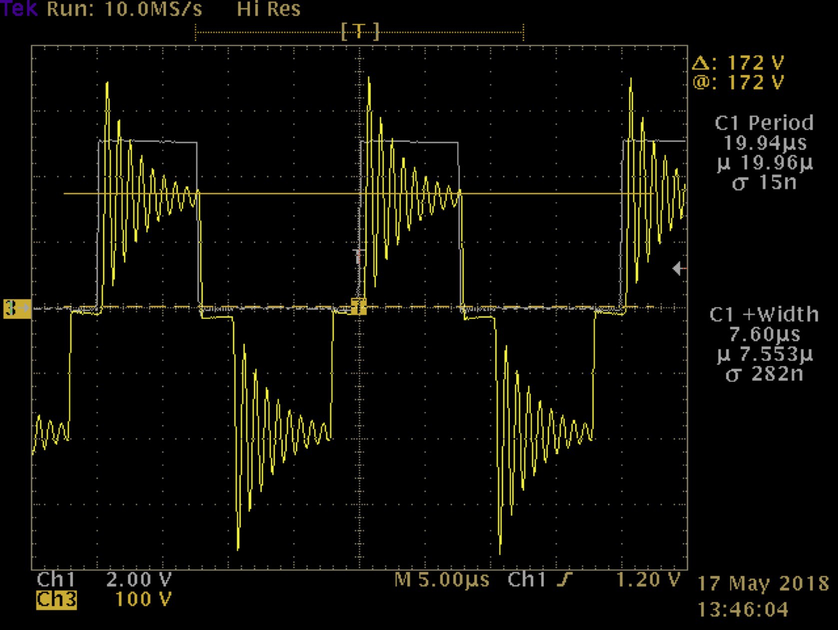
Above is the waveform at the anode of one of the rectifiers with a 1A load applied. Note the scale for CH3 - 100V. The cursor marks the 'no ring' expected voltage. The amplitude of the first ring cycle is nearly 200V! Even with 35nS reverse recovery times and generous thermal pads the rectifiers run hot (>50C) due to the ring. High loads make it worse. Higher input voltages make it worse. Of course this ring is reflected to all the windings. It renders my primary current sense circuit useless. It’s amazing the thing runs at all. After mucking with it for a few hours it’s obvious that a transformer rebuild is required or the design is DOA.
So started a two-month journey to come up with a working transformer. Along the way I earned another degree from the school of hard knocks: when designing a power supply - any kind - always start with the transformer. I had done this but with an inadequate working knowledge of high voltage windings.
I built-up another copy of the full bridge board used in the TS50 (easy to swap transformers) and proceeded to test a dozen different builds using RM & toroid cores with a variety of winding configurations. Interleaved, bifilar, interleaved & bifilar, foldback, single layer, a combination of all of them. Faraday screens too: for both primary & secondary. But it didn’t matter - the results were consistently bad. The ‘best’ design had a measured lumped parasitic capacitance of 10nF and the worst greater than 130nF but in-circuit their performance was almost indistinguishable: a resonant ring with a peak amplitude greater than 100V above the design voltage with a decay lasting the entire duty cycle (5-90%).
The frequency of the ring was a clue. It was over 1MHz but the lumped capacitance should have produced a much lower (100-500kHz depending on the build) resonant frequency. Winding-winding capacitance was ~ 300pF which is more in line and the screens should have helped but didn’t. That left me with turn-turn capacitance which is dictated by the permittivity (dielectric constant) of the magnet wire which is, in turn, determined by the insulation used. MW35-C HY is the only spec available on the consumer market that meets the permittivity & temperature requirements so switching wasn’t an option.
I took a step back and went thru all the designs I had tested. Conventional (non-CT) windings didn’t ring. I found one of the 48V builds I had done for the original inverter work but hadn’t used. It had a center tap so I tested it. Casual observation showed no ring but a closer inspection of the waveform showed the same characteristic ring but at a small (<2V) amplitude. I had been speculating for some time now that the volts per turn, along with the turn-turn capacitance, were the cause of my pain and this was evidence. In a center-tap design one leg of the winding is conducting on each half cycle; the other leg is pulled negative. So on my 48V build the voltage across the rectifier anodes is 96V. On the transformer for the TS350 with a 170V output, the voltage across the rectifiers is 340V.
It was really hard to find literature that speaks to this phenomenon but I did manage to find a few articles. One from TI and another from an academic and both confirm that building high-voltage center-tap transformers is problematic. The large voltage gradient across turns, combined with the turn-turn capacitance, can induce a large resonant ring. To prevent this the progressive (or bank) winding technique is used to wind the high voltage secondaries. I’ve seen a few variations to this but essentially it requires that what would be every other turn in the layer be wound above the previous in a second layer:
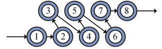
This significantly reduces the voltage gradient and hence the amount of capacitive energy stored. I made several attempts to build a transformer with this technique but doing so by hand and without specialized tools, even with 20AWG wire, was impossible.
So back to square one. I could build a full bridge DC transformer (no CT) but, how to build a practical inverter and regulate the AC output?
Option 1: employ a buck stage in front of the full bridge, similar to the TS50. Possible but, like the TS50, this adds components & complexity and introduces more losses. Because it’s important for the inverter to operate off of 12VDC supplies it must be able to function at rated output down to at least 11VDC. At that voltage the buck stage must function like an LDO but with almost no voltage drop which is impractical. The primary currents are very large (<50A) which will dictate a large inductor. Last, the buck stage could impede the inverter’s ability to properly respond to inrush & transient demands generated by the AC equipment it’s powering.
Option 2: move the buck stage to the high voltage side. This solves the loss / LDO issues of #1 but there’s still the complexity of the added stage and transient response. The design must also deal with higher voltage stress which will likely increase losses.
Option 3: regulate the AC amplitude directly in the sine stage. This is done by sensing the voltage and adjusting the sine table values. No additional power stages are necessary and only a few additional components, and it can be easily adapted to the existing design. It also eliminates the filter inductors in the secondary supplies. The downside is a more narrow input voltage range of 11 - 15 VDC since the sine bridge voltage will float in proportion with the input voltage (e.g. a 15V input equals 240V secondary). Without getting too expensive, the selection of 300V MOSFETs is much better.
Option three is where I am. To make sure there are no surprises I’m hacking the existing TS350 build. Read the logs, avoid my mistakes, and borrow as you see fit.