Objective. A design goal for TS350 was to leverage a single current sense circuit that could provide both pulse-pulse, or Safe Operating Area (SOA), protection and average / RMS current for power management. Cost and space were key drivers. I prefer to use current transformers because of their inherent low noise, galvanic isolation, and undistorted output, but in this design they don’t support the objectives. First, they are relatively large. More importantly, using a single CT for both sides of the bridge with a high fixed duty cycle won’t provide sufficient time to reset the core without flyback voltages in excess of 200V. To avoid this I’d need to use two and that would require additional downstream circuitry.
Current Sense Design. A high-side sense resistor and differential amplifier are used for current sensing. Compact and cheap. The trade-off is a not so clean signal that requires downstream conditioning. I opted for high side sensing to avoid / reduce the incidence of problems associated with COM below ground for the gate driver.
Reference the schematics posted to the project to follow this description. R307 & R308 are paralleled to form the sense resistor. Their paralleled value of 1.5mΩ produces a differential voltage of 1.5mV/A. U302 is a TI OPA197 rail-rail, high speed Op Amp. R316 sets 10x gain for an output of 15mV/A and, Q305 level shifts (removes the INV_(+) supply voltage) the output for direct processing by the MCU, U101. R311 & R312 provide current limiting and in conjunction with D302 & D303 protect the Op Amp from voltage spikes. C314 & C317 provide local bulk capacitance and decoupling. Note that the supply voltage for the Op Amp is the direct input voltage and not the inverter auxiliary supply (VCC_INV). This is necessary for it to function - it’s inputs can’t be at higher voltages than its supply. This will be true for the redesign as well.
SOA Protection. The image below depicts the MCU’s peripheral configuration that performs both SOA and current averaging. Comparator CM2 is responsible for SOA protection. It’s positive input is connected to voltage reference DAC1 to define the over-current limit (in the prototype the limit is set to 140A). The negative input is connected to the external current sense circuit’s output. Ideally CM2’s output would connect directly to COG1 to drive a Falling Event (FE) input to terminate the drive pulse but it was previously mentioned that signal conditioning is required.
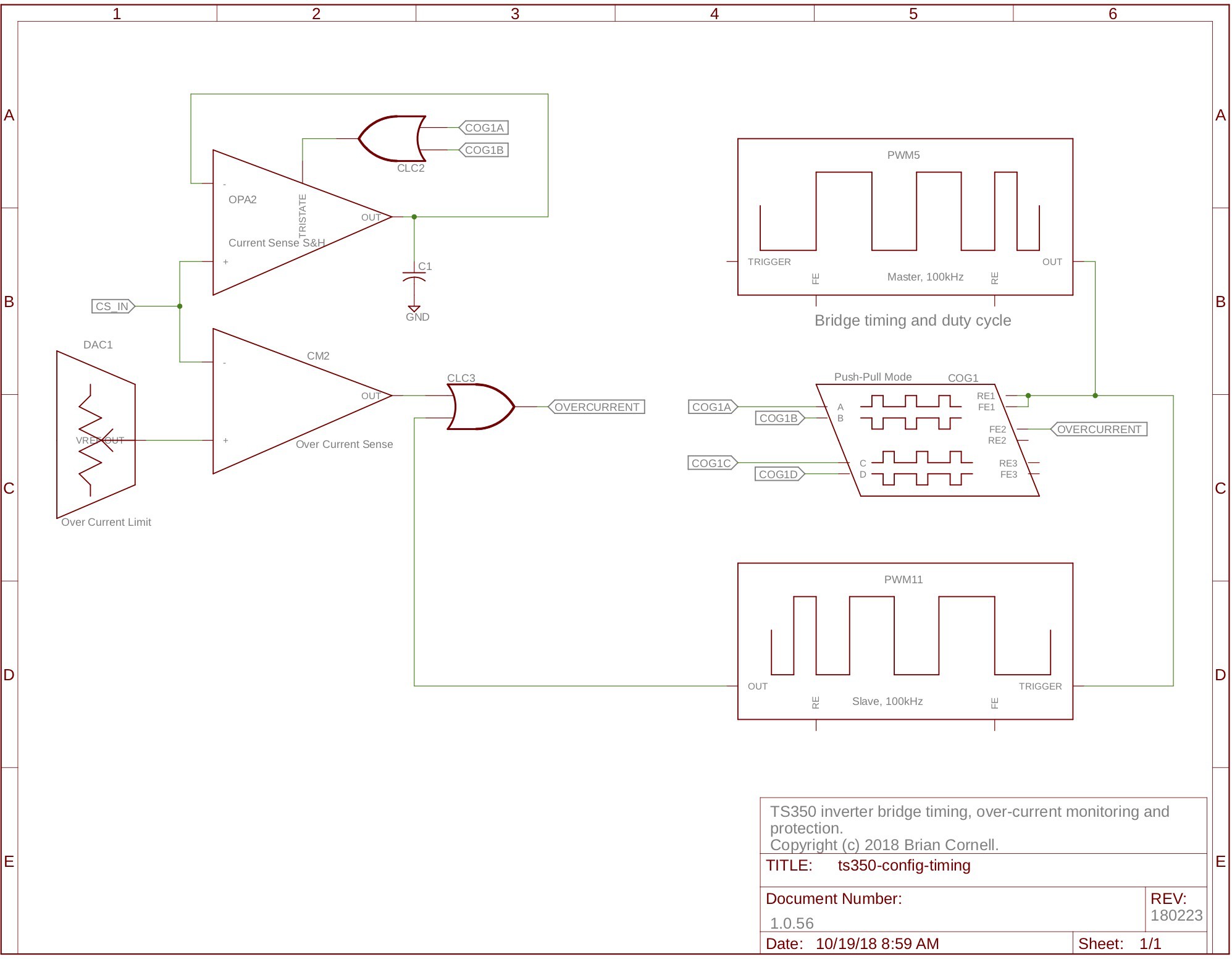
In this figure channel one is the output of the current sense circuit with a peak current of 48A. The ideal waveform would be the ‘ramp on a step’ (trapezoid) with no +/- spikes. The curved leading edge is due to the rise time of the Op Amp. Some of the positive spike at pulse termination is due to probe parasitics (as is the ring at pulse start) but much of the negative spike at pulse start is real. This created problems that the COG’s native blanking feature couldn’t handle (the MCU would reset). The redesign will incorporate a protection diode across the sense input to ground but even that may not be sufficient given the pulse amplitude.

A more flexible blanking circuit was fashioned using MCU peripherals CLC3 and PWM11. The PWM is slaved to the master, PWM5, and set to the same frequency. PWM11’s duty cycle defines the blanking time. CLC3 will only allow a FE outside of the blanking time. It is possible for a FE to occur at the end of the DC but that is non-consequential since the master PWM has already terminated the pulse with a FE.
The firmware protects the inverter from continuous over-current events. When running, COG1’s duty cycle is sampled on each pass of the run loop. A simple PID filter sets the limit on time & rate (integration is somewhat variable based on loop timing) of over-current events and when exceeded the inverter is stopped.
This design is quite effective and has demonstrated ability to protect the bridge with the transformer secondary shorted. I have not tested it’s ability to protect against a dead short on the primary but I’d expect that the bridge would fail since this circuit can’t respond fast enough (it relies on the protection that the transformer’s inductance affords - the inability for current to change instantaneously).
Averaged Current & Power. MCU peripherals OPA2 (Op Amp) and CLC2 form a sample & hold circuit. OPA2 is configured as a voltage follower with its inverting input connected to the current sense circuit’s output. A nice feature of these Op Amps is the ability to tristate their output. CLC2 drives the tristate control. It’s inputs are connected to the high side gate drive of each side of the bridge. Hence, OPA2’s output is only active when the bridge is being driven. The voltage across C1 represents the average of the current sense signal and can be used to derive the RMS input current and power; and from this the output power can be estimated.
The run loop continuously samples the inverter’s input voltage and the voltage across C1. The current & input power are calculated using the average of several samples. In the prototype firmware a fixed adjustment factor is applied to the current sense value to compensate for the slope of the current sense signal; I might revisit this since the compensation isn’t linear over the load range. Like over-current, a similar PID filter is applied to limit power.
Performance. The prototype firmware only calculated input power since I knew that a revised design would alter the model. To test, an electronic DC load was used to load the inverter’s high voltage secondary instead of using an AC load for a few reasons. First, it’s more difficult to obtain a precise AC load with the equipment I have. Second, and more important, is that the current on most all AC loads will vary in amplitude which complicates the measurements. The DC load is precise. A hall effect current sensor, in series with the inverter’s DC power source, measured current, and it’s output was connected to a scope that calculated the RMS value of the signal. A DMM measured the voltage at the inverter’s relay supply connections (same measurement points as MCU’s measurement).
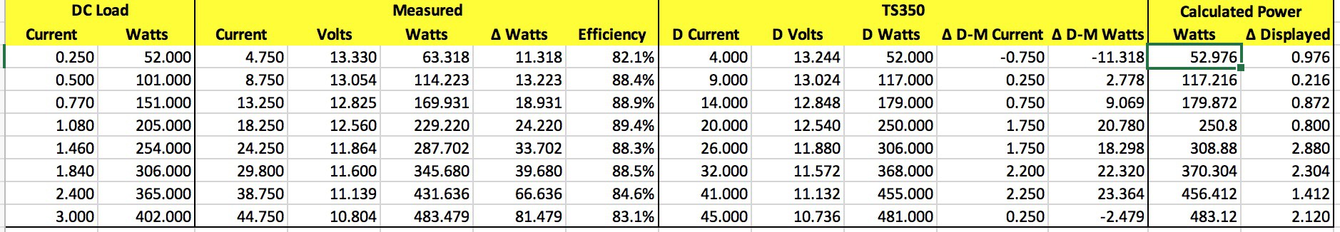
The grid shows how the TS350 did. The TS350 ‘D’ columns are the values taken from the console ‘monitor’ command. The measured voltages track well with those acquired by the controller. The efficiency isn’t great but trends as expected. Interestingly the delta current / power curves have the same shape. I expected the deltas to remain constant, or increase as they do at the 306W / 365W loads. I suspect it’s due to OPA197’s rise time: at high loads the slew rate becomes a significant factor.
The revised design will need to employ a correction formula or table for input current & power as well as output power.
Discussions
Become a Hackaday.io Member
Create an account to leave a comment. Already have an account? Log In.