 Jan Waclawek
So storing energy for RTC in a PP foil capacitor, utilizing its high-voltage properties, would mean to build something like this (the controlling mcu, as proposed to be STM32L476, not drown here):
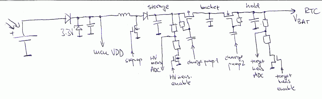 The solar panel on the left would keep charged a low-voltage capacitor, and the mcu would be powered from that point. That's why a 3.3V Zener is added, to avoid overvoltage. This is the simplest arrangement, although different ones are certainly possible, allowing that point to go as high as the solar panel would go and powering the mcu through a 3.3V LDO capable of efficiently bypassing itself on low input voltage (this unfortunately is not an often advertised property of a LDO, so this may need investigation, too, and maybe some more innovative circuitry). Another possibility is to use a series resistor and a shunt regulator (or simply a Zener diode) for supplying the mcu, or a more or less sophisticated step-down. The mcu is not going to execute too much code, and is anticipated to run in a power-efficient mode, with power consumption probably way below 1mA, so the series resistor-Zener combination may be entirely sufficient.
The front-end could involve also a standalone "harvesting-optimized" step-up, so that operation can start at sub-volt outputs of the solar panel - the chosen mcu starts at 1.8V. But this in practice is not such an issue, as solar panels can be connected in series to boost their output voltage at low illumination, if needed.
The mcu, when input voltage allows it to run, would measure the current state of charge of the "HV storage" capacitor by switching on the divider and measuring the voltage on it; then, as necessary, it would start pulsing the output driving the step-up transistor. From occasionally measuring the input and output voltage of the step-up, the mcu can calculate the needed number of "boost pulses" to reach the maximum design voltage of the "HV storage" capacitor, and then simply let a timer to produce the needed pulses, while the rest of the mcu can go to power-efficient "sleep".
While the "HV storage" capacitor charges, on the load side, measurement of the HV voltage and target/holding capacitor volrage before and after a transfer of "bucketful" of charge provides the calibration data needed for running the step-down when primary power is not available. These have to be stored somewhere - the lowest consumption "Shutdown" mode of the mcu, the RAM is powered down and does not retain its content. So, during/after calibration, the data need to be stored in the FLASH (which, given the modern 32-bitters don't have an integrated EEPROM is sort of an annoyance, causing the program stop for the duration of write, and also presents surges of relatively high power consumption); in an external EEPROM or similar (which again is an annoyance, as we need these data during low power operation, thus we don't want to power an extra IC nor want we to burn power during the lengthy communication with it); or, the best solution, if there is not too much calibration data (i.e. if we can piecewise linearize the data or find a simple algorithm to calculate needed pulse rate, given certain state of charge of the "HV storage" capacitor, and calculate how this charge changes in time), we can store them in the 32 32-bit Backup Registers which are part of the RTC and are powered together with RTC.
When primary power ceases, the mcu has to calculate the next period after which stepdown has provide a "bucketful" of charge to the holding capacitor, program the RTC to wake up the mcu after this period, and go to the "Shutdown" mode. After waking up, this process has to be repeated. From time to time, the mcu might need to measure the state of charge of the "HV storage" capacitor and maybe also the state of the "holding" capacitor, to readjust for any drifts.
As the mcu has to be powered during the no-primary-power period together with the RTC, both the RTC power supply pin (VBAT) and the mcu power supply pin (VDD) have to be connected; so the internal switch which isolates VBAT from VDD while VDD is low, here can't be used. The "mcu VDD" and "VBAT/RTC" nodes in the schematics above in fact represent "high-power-VDD" and "low-power-VDD", and are to be connected through a low-leakage swithing fabric - maybe merging them through two low-leakage diodes would suffice, as the currents involved are low. There also has to be also a means to notify the mcu that there is sufficient "high power" - one way to do this would be to use a voltage detector IC (traditionally used to provide reset in past times when voltage detectors were not commonly built into mcus) connecting its output to a digital interrupt input of the mcu (the raw input volage can't be used, as voltages around VDD/2 on digital inputs may cause increased power consumption).
It is clear that such a project, involving both nontrivial electronics and nontrivial software, with a bunch of unknowns ahead, is not something one is going to whip up during a couple of spare weekends between workdays paying the bills. So, at this point, I was about to give up...
Discussions
Become a Hackaday.io Member
Create an account to leave a comment. Already have an account? Log In.