Have you ever done a project that was supposed to be quick & simple, but instead takes on a life of its own, you're never satisfied, and is never done? For me that's Timer.
It started out as a solid state design to replace the crappy electro-mechanical timers used for decorative lighting. While cheap, I got tired of replacing them because of exposure to the elements. All I wanted was a timer to run 24h cycles that was weather proof, could switch light loads., and would last forever. Here's the prototype.
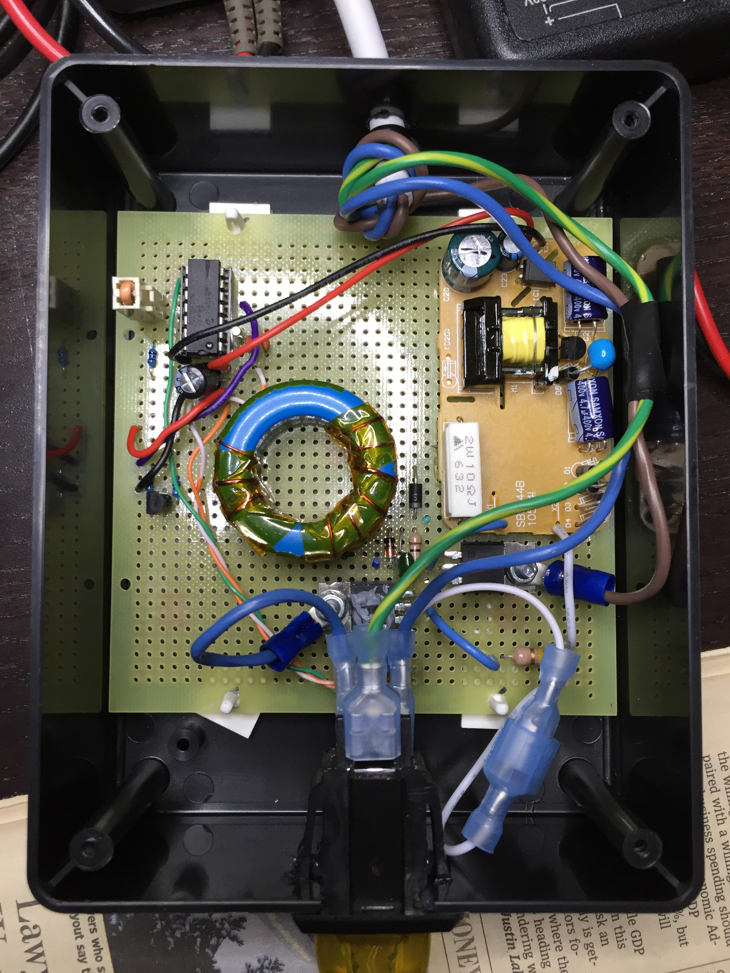
It had a jumper to set a 4/8h on cycle. The giant toroid (all I had on hand) is for the isolated gate drive in the MOSFET based solid state relay (SSR). It used a PIC16F616 controller and could handle a 2 amp load. The board in the upper right is a 5V logic supply hacked from a phone charger. Worked great but not too flexible and certainly not weatherproof.
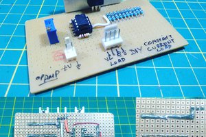
Miniaturizing & weatherproofing went pretty quick but then I kept wanting more: more features, higher loads, how much can you do with a timer? Apparently a lot because two years and few dozen iterations later I've taken the design in its current form about as far as it can go. A reboot is in order which is why I've marked this as an on-going project. But it's not a priority for me right now so it will take a while.


 Inderpreet Singh
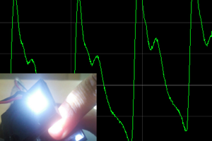
 Jithin
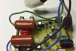
This project is genius. I often wish I had something to make my old Samsung clothes washing machine turn on when I was at work to clean my clothes when I was away, because it was so loud I preferred to be out of the house when it was on. My friend works for Appliance Repair Waco so I'm going to pass this on to him and see what he thinks. This could end up on Shark Tank or something. All the best!