 jean
jeanI thought I'd make this one more of a process log, showing some of the experiments and iterations along the way.
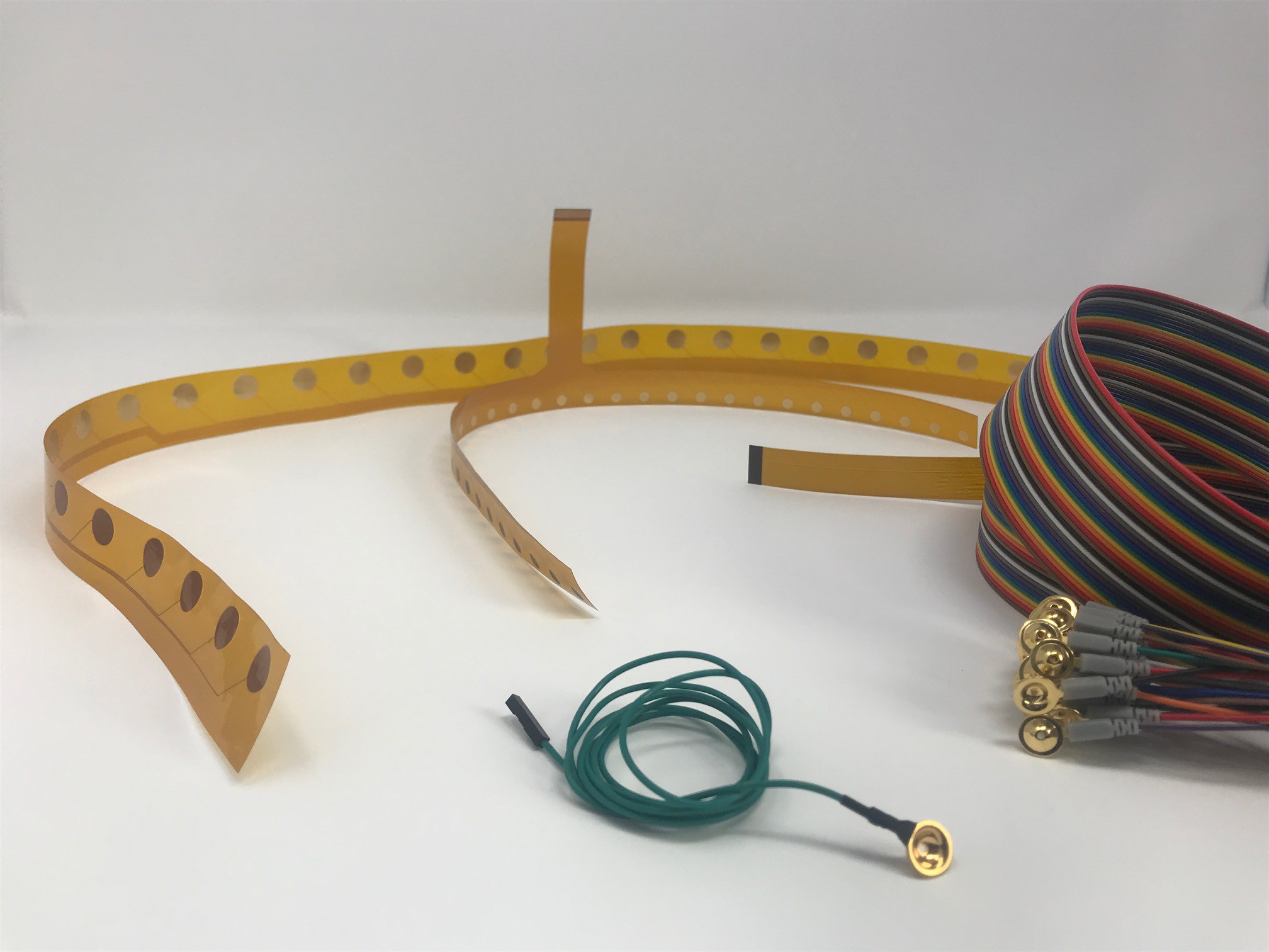
The idea of using a flex PCB as an electrode cable seemed efficient, as nobody likes having cables go everywhere and having them be the wrong size for your needs. This is both a good and a bad idea. It works great in tanks and I believe this is a superior method when doing reconstructions in phantoms, and it also works on the body. The problems with flexPCB's come when you encounter a concave location on the part of the body you are imaging. For instance the dibit that your backbone makes around your thorax. To get over this, I also made the 32 electrode cable which you see here on the lower right - I am yet to try it as it just arrived but it appears like it will be a good solution to the concavity issue.
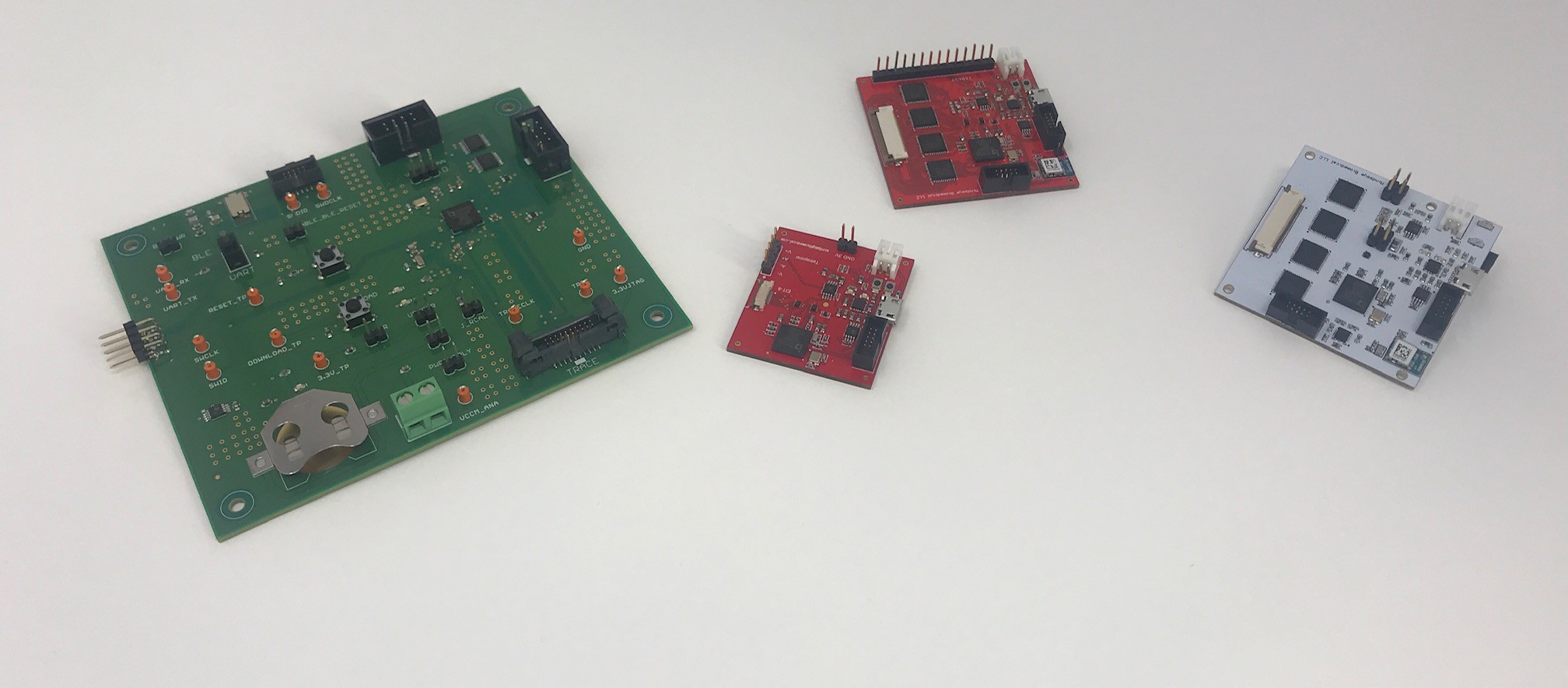
PCBs aren't born perfect it turns out and it took a few attempts(and I still have one more final run planned actually). On the left you can see my initial attempt which worked for 8 electrode EIT but had a couple of small errors. It's not as user friendly as the design on the right but has bluetooth and lots of options and test points not to mention being a bit on the large side! The second smaller board was one made just to do 8 electrode EIT as well as bio-impedance spectroscopy. The third board shows my move to 32 electrode EIT. At this stage I decided to do another run which was all about user friendliness and fitting neatly into a box with a battery which is the white PCB on the right. I made a small mistake in the FTDI chip arrangement, which means I need another run, though this PCB works in most regards(the analog sections and the bluetooth as well as the power sections are all good). The next iteration will have the FTDI chip fix as well as a few more added tests points.
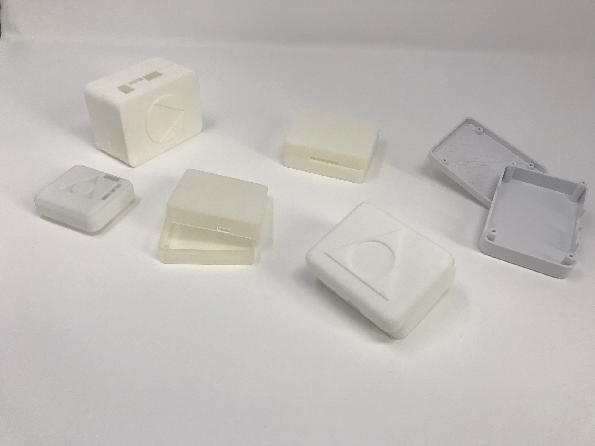
Finally we have the boxes - it's always nice to have an enclosure which both protects the PCB and houses the battery. Mechanical design is not my forte and here are a few attempts. I started with a transparent design(the yellowish looking thing on the left bottom) an decided transparent 3D printing is not the way to go. The large one on the left was a bit overly generous with space and it's nicer to have something snug. The one on the far right, was not done with ABS but PLA instead and you can see how rough the finish is on that. It's so rough the screw holes aren't functional. Then, there is the one at the bottom which fits snug, is relatively smooth and does the job!
Discussions
Become a Hackaday.io Member
Create an account to leave a comment. Already have an account? Log In.