 Blair Vidakovich
I received some constructive criticism about the Flip-Flops I am using the construct the various elements of the RAVEN. I think a lot of the apprehension other hackers have about the R201 DEC Flip-Flop I am using is because it contains a great number of circuit elements -- if these circuit elements were in a large part active during Flip-Flop operation, then obviously the R201 would be very slow.
In this log I'd like to clean up and and explain exactly how the main Flip-Flops in the RAVEN will function. I do not believe these DTL Flip-Flops I have lifted from DEC R-Series Logic are slow, and will result in less than 1 MHz performance.
The Most Basic Element of R-Series DTL Logic
The most basic circuit element of any electronic digital logic is the inverter. This is the basic inverter of the DTL logic that the RAVEN uses:
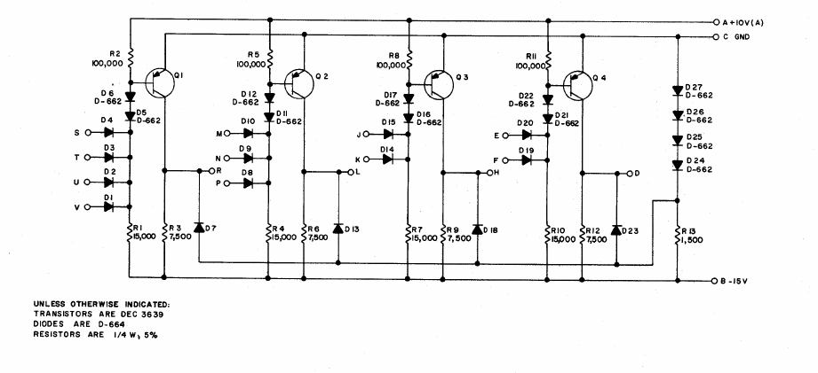
 A couple of examples can be provided which show the actual way this inverter is implemented in R-Series Flip-Chips:
The R113 Diode Gate
The R121 NAND Gate
R-Series digital logic specifies -3V as logical ONE, and 0V/Ground as logical ZERO.
Inverter Simulation
Conventional current flows up through the emitter of the transistor, and out through the collector. Depending on whether there is 0V/ZERO or -3V/ONE at the INPUT terminal determines whether current will flow out through the base of the transistor and cause it to saturate.
-3V/ONE at the INPUT terminal will reverse bias the INPUT terminal diode, and open up a path for current through the transistor base up through the -15V terminal past the steering diodes. The transistor will then conduct, and the voltage at the output terminal will be 0V/ZERO, effecting an inversion.
0V/ZERO at the input terminal will cause the INPUT terminal diode to become forward biased, making the current path through the transistor base a path of much higher resistance. A small amount of current still leaks through the base through to the -15V terminal near the INPUT, but it is not enough to turn the transistor on. The transistor stops conducting and the voltage at the output terminal is therefore -3V.
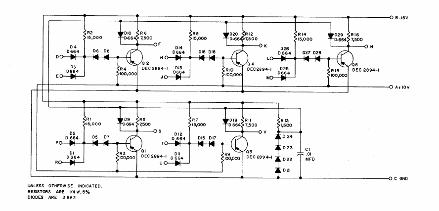
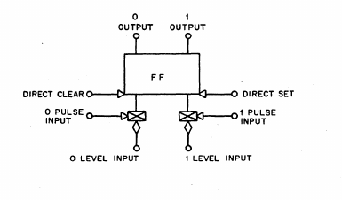
R-Series Logic Flip-Flops
The simplest Flip-Flop of the RAVEN is two Inverters complementarily connected together like so:

As you can see, this is the heart of the R201 Flip-Chip:
What, then, is the rest of the circuitry in this schematic?
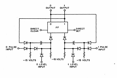
Diode-Capacitor-Diode Gates
The answer is that the extra circuitry is 'Diode-Capacitor-Diode' gates. This circuit element is a very innovative and useful solution for both (a) edge-triggering; and (b) constructing JK and D Flip-Flops is as little circuitry as possible.
This is the basic DCD gate:

The basic principle behind this circuit is that the capacitor charges and remains charged so long as the PULSE INPUT is held at -3V, and the LEVEL INPUT is held at 0V.
When the LEVEL INPUT equals 0V, and the positive edge of a PULSE INPUT signal changes from -3V to 0V, a positive voltage is generated at the output, which serves as a trigger for a Flip-Flop.
When LEVEL INPUT = -3V and PULSE INPUT changes from -3V to 0V, no such positive pulse is produced.
See the following simulation:
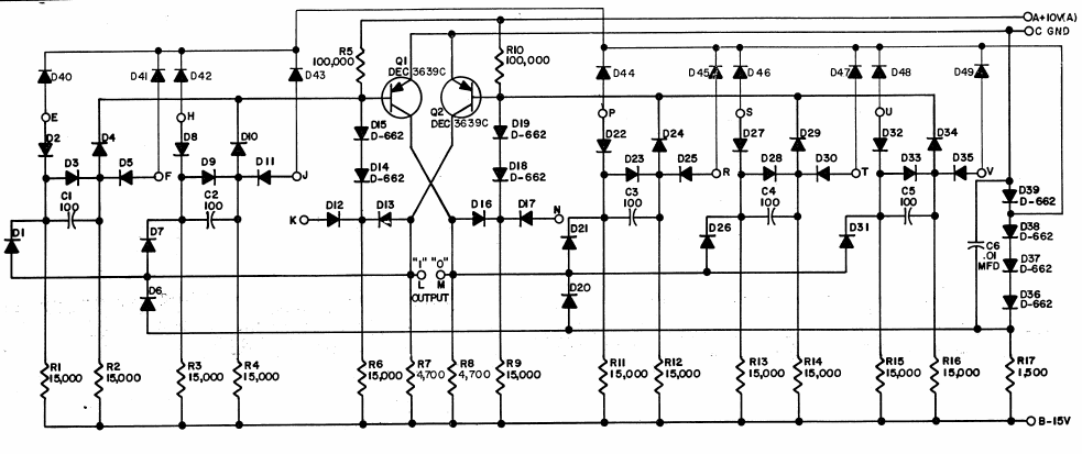
Creating D and JK Flip-Flops
The process of creating complex, clocked, edge-triggered Flip-Flops is as simple as preparing the inputs to Flip-Flops attached to DCD gates. The following two schematics are isomorphic/identical in meaning:
A JK Flip-Flop can be constructed by simply sending identical pulse inputs to a DCD-gated Flip-Flop:
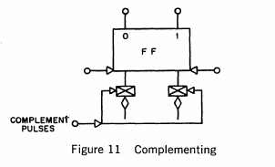
So long as the LEVEL INPUTS are tied to ground, identical PULSE INPUTS will cause a Flip-Flop to complement.
This simulation demonstrates a JK Flip-Flop constructed from a DCD-gated Flip-Flop:
This serves as the basis for this Up-Down Binary Counter Register:
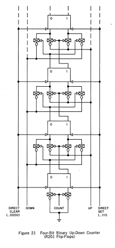
Binary counting is therefore achieved with the minimum number of circuit elements, as well as minimum number of transistors!
The exciting thing about DCD gates is that they allow logical isolation - meaning one does not need to resort to using Master-Slave Flip-Flops in order to clock some Flip-Flop element. Logical isolation from input and output is achieved by DCD gates, which allows the component count to be reduced dramatically.
Discussions
Become a Hackaday.io Member
Create an account to leave a comment. Already have an account? Log In.