 SHAOS
SHAOSTERNARO is planned to be a hybrid integrated circuit working as FPGA-like ternary device with binary control (because nobody invented ternary serial memory yet) that has 9 general purpose ternary IO pins. First prototype of TERNARO in DIP24 package will not be able to read bitstream from external serial memory yet as other FPGAs do. Instead we will need a regular binary microcontroller to feed TERNARO with stream of bits through slave SPI interface to program it after power-on:
         ___________
        /     U     \
 IO1 --|1          24|-- TA0
 IO2 --|2          23|-- TA1
 IO3 --|3          22|-- TA2
 IO4 --|4          21|-- TA3
 IO5 --|5          20|-- TA4
 IO6 --|6  TERNARO 19|-- TA5
 IO7 --|7          18|-- TA6
 IO8 --|8   DIP24  17|-- SDO / TEST
 IO9 --|9          16|-- SDI
Vneg --|10         15|-- SCK
Vref --|11         14|-- /PRG
Vpos --|12         13|-- /RES
        \___________/
Below you can see description of TERNARO pins for that DIP24 package:
pin 1 - IO1 (general purpose ternary IO)
pin 2 - IO2 (general purpose ternary IO)
pin 3 - IO3 (general purpose ternary IO)
pin 4 - IO4 (general purpose ternary IO)
pin 5 - IO5 (general purpose ternary IO)
pin 6 - IO6 (general purpose ternary IO)
pin 7 - IO7 (general purpose ternary IO)
pin 8 - IO8 (general purpose ternary IO)
pin 9 - IO9 (general purpose ternary IO)
pin 10 - Vneg (common ground connected to chip substrate)
pin 11 - Vref (intermediate voltage level between Vneg and Vpos)
pin 12 - Vpos (common power +5V)
pin 13- /RES (reset of Slave SPI and clear configuration memory)
pin 14 - /PRG (programming enabled through Slave SPI)
pin 15 - SCK (input clock for Slave SPI)
pin 16 - SDI (serial data input for Slave SPI)
pin 17 - SDO (serial data output from Slave SPI if TA=0) or TEST
pin 18 - TA6 (test address bit 6)
pin 19 - TA5 (test address bit 5)
pin 20 - TA4 (test address bit 4)
pin 21 - TA3 (test address bit 3)
pin 22 - TA2 (test address bit 2)
pin 23 - TA1 (test address bit 1)
pin 24 - TA0 (test address bit 0)
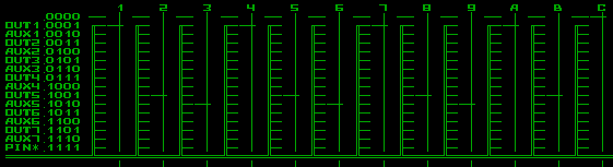
Chip will allow to read up to 128 internal ternary points for debug purposes (testing point is chosen by TA0...TA6 address bits) that is connected to TEST output (which is used as SDO if all TA bits are grounded).
Internally TERNARO will have 7x9 grid of ternary configurable logic blocks as one showed below:
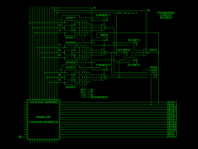
Analog interconnect will electrically connect every vertical line to nothing or only one horizontal line (line 15 is an external pin and lines from 1 to 14 are connected to 7 logic blocks in that row):
Every such interconnection block will be configured by 6 bytes (every 4 bits say where every vertical must be electrically connected in the channel while 0000 will mean no connection) and every logic block is configured by 4 bytes:
Byte 0 - 1st selector:
 bit 0 - input N of 1st selector
 bit 1 /
 bit 2 - input O of 1st selector
 bit 3 /
 bit 4 - input P of 1st selector
 bit 5 /
 bit 6 - make 1st selector E21 (XXY1)
 bit 7 - make 1st selector E12 (XYY1)

Byte 1 - 2nd selector:
 bit 0 - input N of 2nd selector
 bit 1 /
 bit 2 - input O of 2nd selector
 bit 3 /
 bit 4 - input P of 2nd selector
 bit 5 /
 bit 6 - make 2nd selector E21 (XXY2)
 bit 7 - make 2nd selector E12 (XYY2)

Byte 2 - 3rd selector:
 bit 0 - input N of 3rd selector
 bit 1 /
 bit 2 - input O of 3rd selector
 bit 3 /
 bit 4 - input P of 3rd selector
 bit 5 /
 bit 6 - make 3rd selector E21 (XXY3)
 bit 7 - make 3rd selector E12 (XYY3)

Byte 3 - additional configuration:
 bit 0 - connect feedback line to form MEM block
 bit 1 - simplification bit SIMP1
 bit 2 - simplification bit SIMP2 (spare input control)
 bit 3 - simplification bit SIMP3
 bit 4 - make 1st selector independent (INDEP1)
 bit 5 - make 3rd selector independent (INDEP3)
 bit 6 - AUX line control (see below)
 bit 7 /

AUX line control configuration:
00 - not connected
01 - 1st selector output
10 - 2nd selector output
11 - 3rd selector output

Input configuration for selectors (bits 0...5 of first 3 bytes):
00 - constant O (neutral)
01 - constant P (positive)
10 - constant N (negative)
11 - through signal
Note: XXY and XYY paired switches depend on each other - if any one of those control bits is 1 then paired switch is also disconnected to free central line of selector...
P.S. And yes, I want to make a real chip prototype on CMOS 0.5um technology as part of Shared Silicon project ( TERNARO will occupy 50% of 2x2mm silicon : )
( it's photoshop by the way ; )