 SHAOS
SHAOSI'm working on TERNARO design since January 2015. Main idea was to design ternary FPGA that may implement any ternary circuit that is built out of bunch of TRIMUXes (like TRIADOR from #Homebrew ternary computer for example). Base element of such FPGA that was chosen in 2015 is 9-to-1 ternary multiplexer:
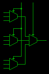
It also may be used as 9-cell ternary ROM with 2-trit address and 1-trit output.
With little re-wiring we can get memory element out of it:
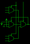
Left-center ternary multiplexer is connected as a buffer (unary function NOP) and it's the main reason why it becomes a memory cell with feedback loop like that.
This is all versions of TERNARO configurable logic block design that I came up with in the last few days and you can see how it evolved in my mind :)
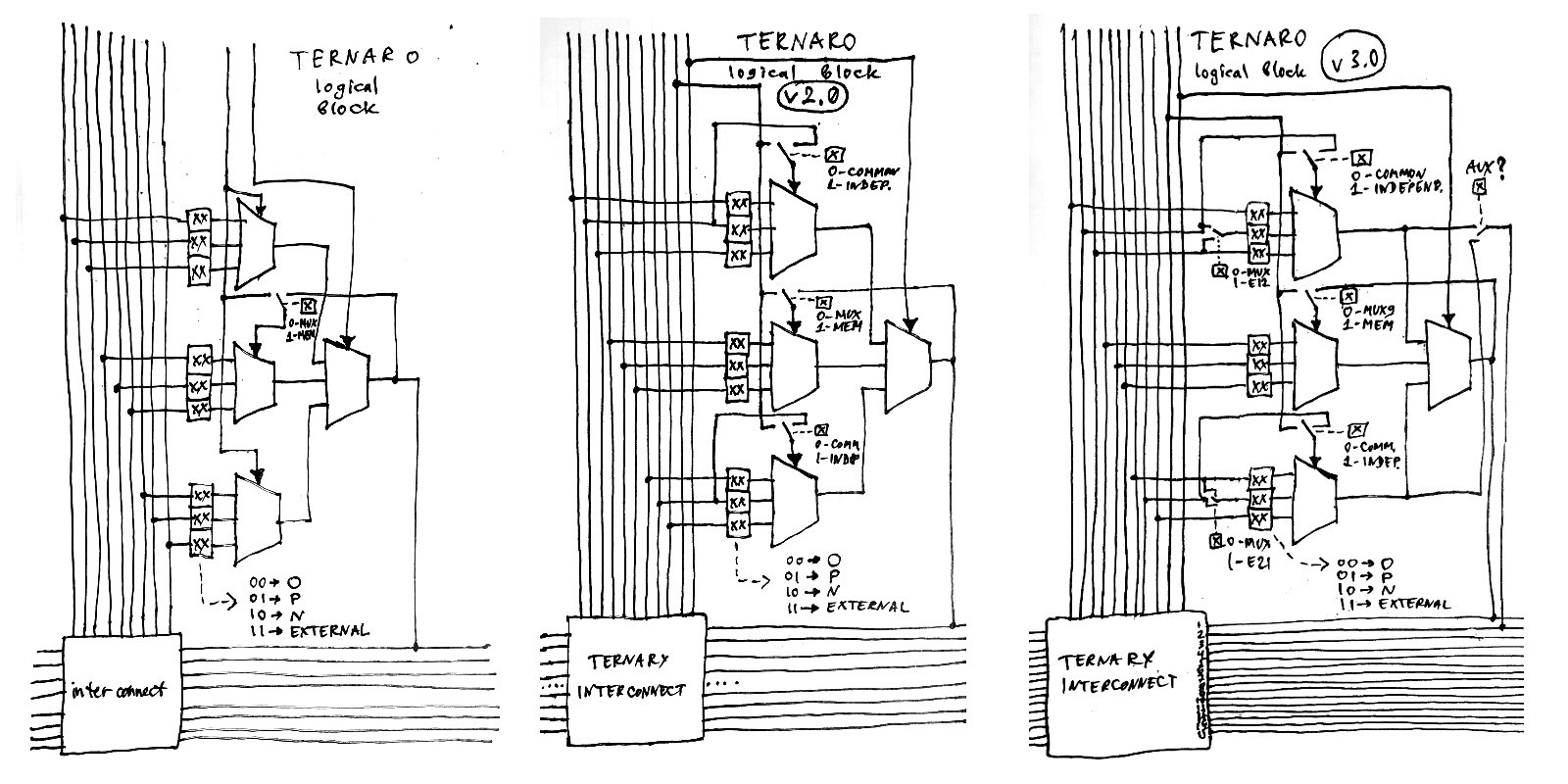
Today version 4 is the last and final design:
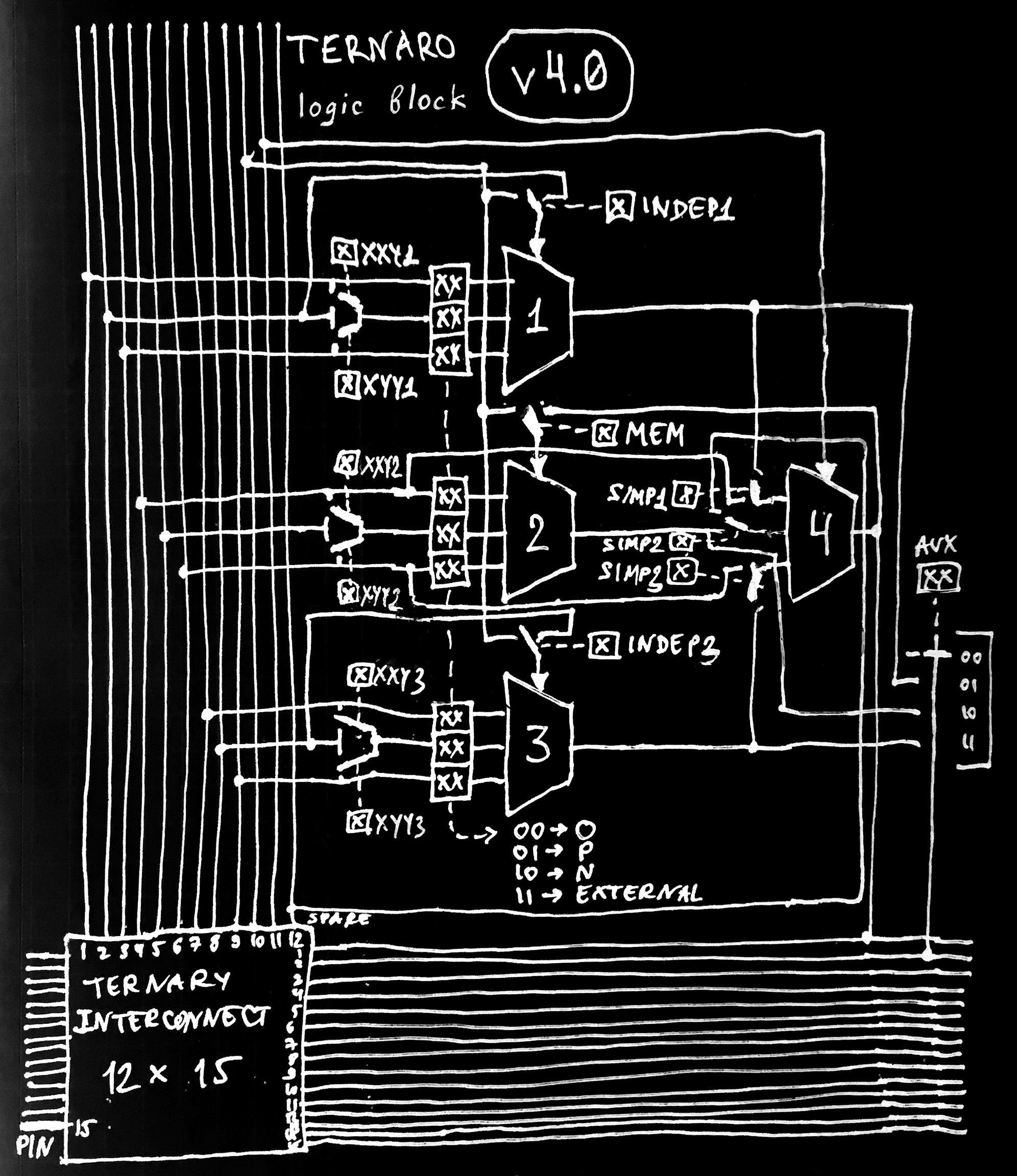
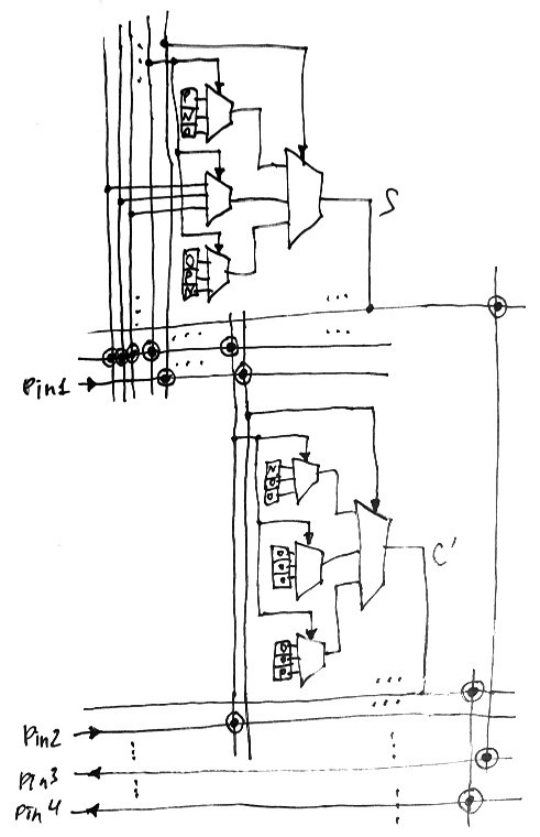
Now 9-to-1 multiplexer may be split to separate 3-to-1 multiplexers. But even with initial programmable capabilities we can easily implement things as ternary half-adder for example:
Also if we have 9 IO pins it means we have 9 horizontal channels with 15 signals in each...
Discussions
Become a Hackaday.io Member
Create an account to leave a comment. Already have an account? Log In.