Recently I found a while to solder and test the latest prototype. All boards have been soldered using a hotplate made from an old iron. The soldering process took about 1 minute, because the iron didn't have a temperature controller to follow the reflow profile. The only thing that prevented burning the boards was a thermostat set around 230 °C. I hope to add a controller soon to improve the performance. There are a few neat controllers on the Internet, this one seems suitable for my needs - https://github.com/makermoekoe/Hotplate-Soldering-Iron
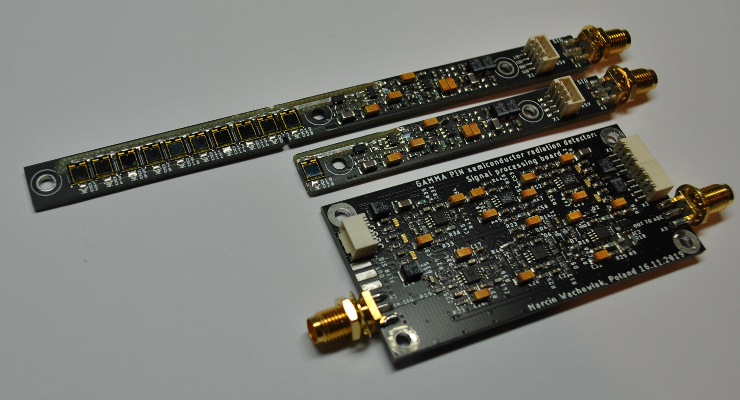
Preamplifier
As you can see, I produced two versions of the preamplifier: one with a single diode and another with a full array of 10. The following results have been obtained using the single diode version as it is less noisy.
The boards turned out to have some flaws but still I managed to get them to work properly.
Issues with the preamplifier board:
- Guard ring introduced to reduce current leaks emerged to be a source of shorting. Exposed traces with components placed upon them were not a good idea. Covering the guard ring with solder mask would render it useless as it is supposed to prevent any currents flowing through surface form contaminations by shunting them to low-impedance node. (topic about it) I may consider to expose only thin edges of the trace and cover the wider areas susceptible to shorting. For the time being I have milled it out to get a functional circuit.
- The second op amp used on the board as subtractor with amplification requires a feedback capacitor to ensure the stability and prevent excitation. It should be around 22-33pF and can be simply placed on the top of the feedback resistor - R17.
- Voltage reference for the subtractor had to be altered to set the output signal baseline as close to the 0V as possible. In my case it required changing the lower resistor of the voltage divider from 92 to 110 Ohms. With such preset baseline of the output signal was at approximately 30mV.
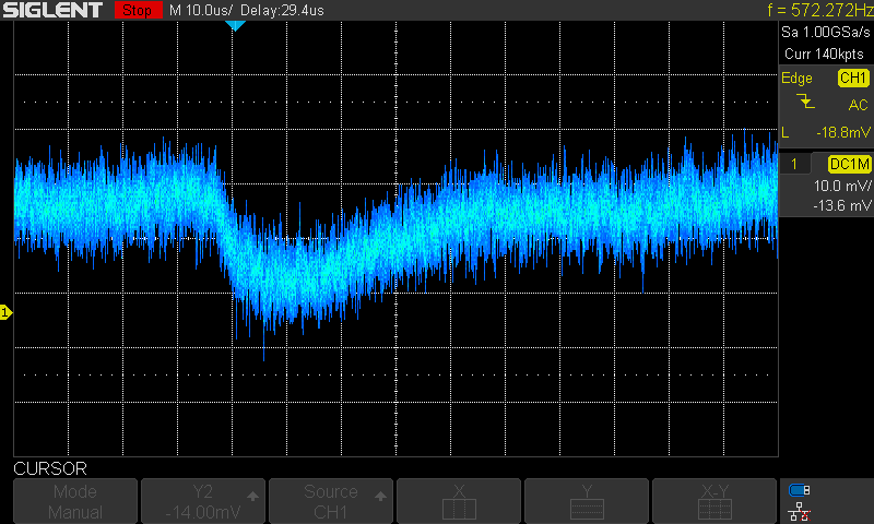
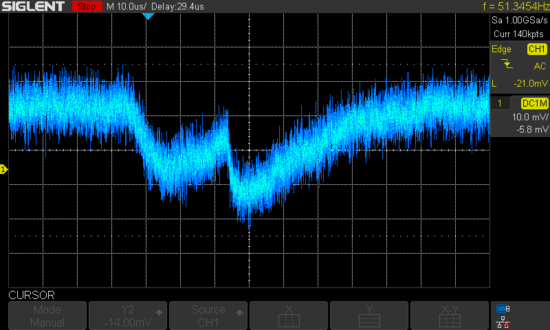
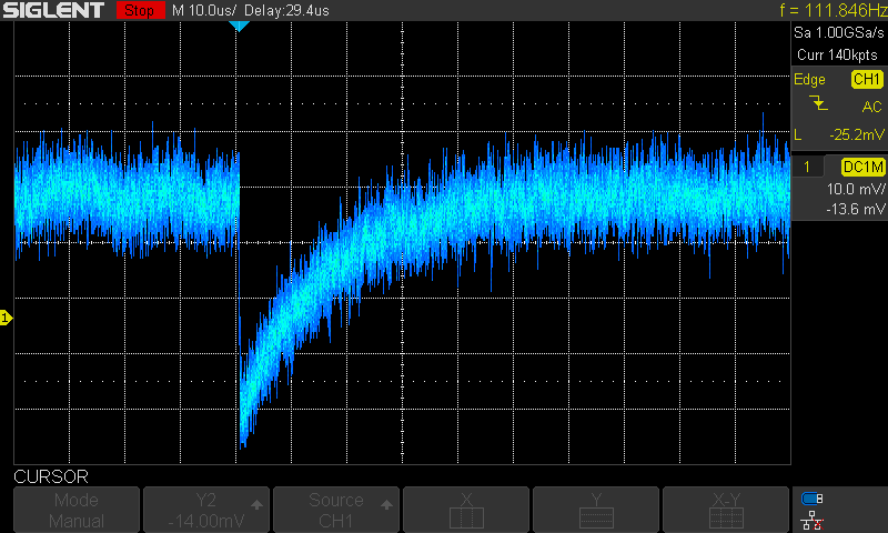
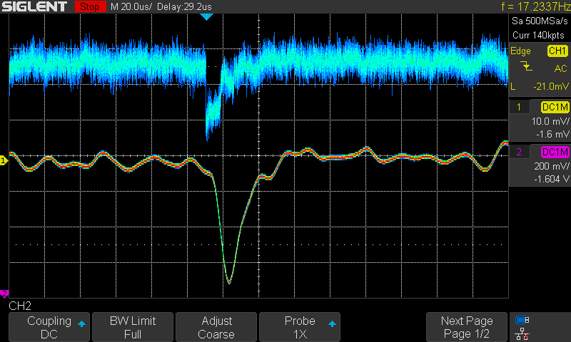
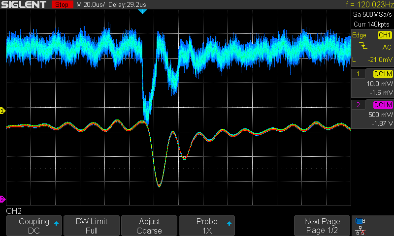
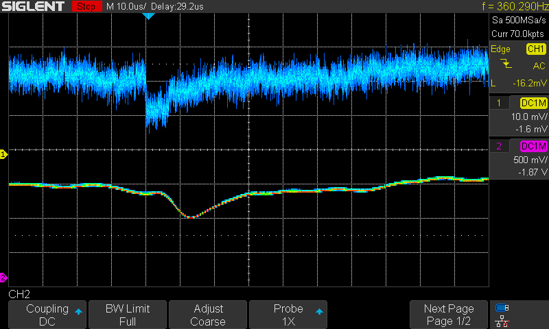
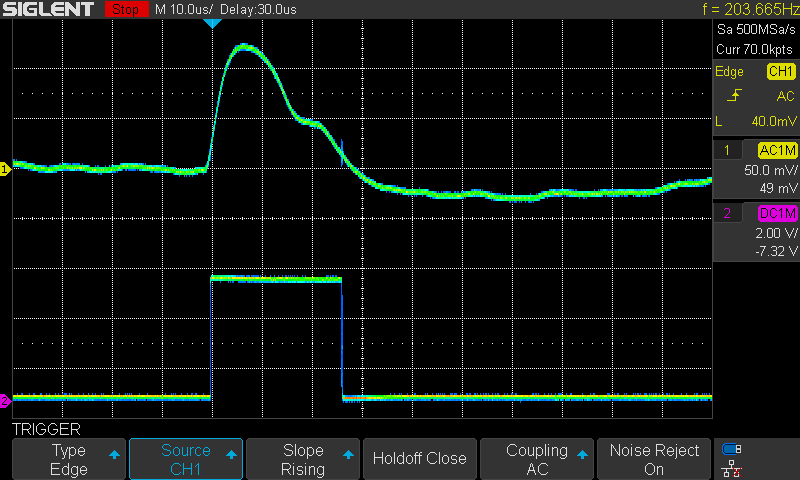
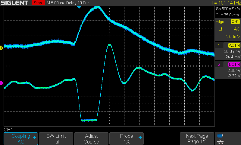
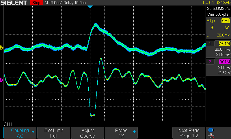
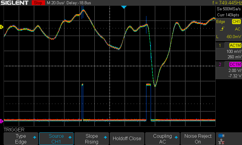
Modified board was mounted in the aluminum box with an Am241 source. This time the diodes were not shielded with copper foil as the box provided enough shielding. Unfortunately, the box was not light-tight so I had to cover the diodes with a single layer of black isolation tape. With that the working point of the TIA was at 2,5V as expected - meaning that there were no additional currents shifting the operating point. Some of the captured screens show the output of the preamplifier:
Signal processing
Having finished a fully functional preamplifier the next step was to process the raw noisy signal with the signal conditioner board. This was definitely more challenging as each segment had to be optimized in regard to the other blocks. Some of the values picked while evaluating the simulation did not provide required stability or operating points and had to be altered.
General issues:
- Resistors or inductors used in power supply filtering need to have low resistance around 1-10 Ohms as any greater value causes unacceptable voltage drop across them.
- Double LED indicators on each side of the board are redundant as they signal the same thing. Only one group should be soldered.
Filter
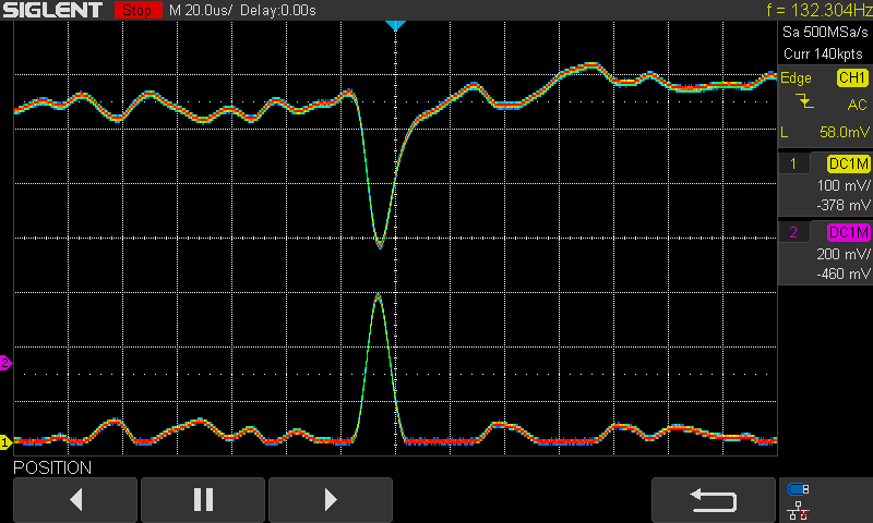
6th order Bessel filter based on Sallen-Key topology may be instable when high gains are set due to required component precision values. In my case I had to reduce the gain of the whole block to 60 and recalculate all values again with ADI Precision Studio. A simple change in the divider at the output of the amplifier will change the gain but the stability of the filter will be decreased dramatically. I also noticed that the filter block was not designed with noise optimization option available in the tool. For any further versions I am considering the 4-stage Multiple Feedback topology with improved stability and proper noise optimization.
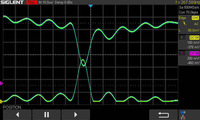
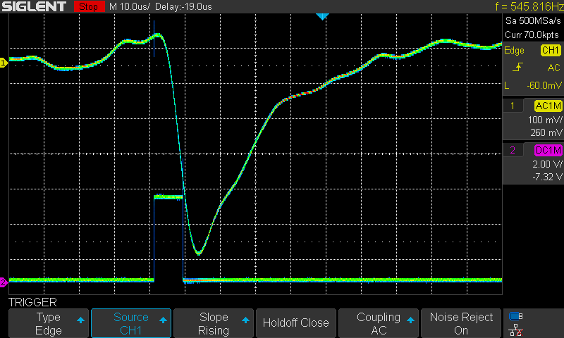
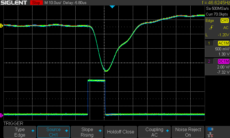
Filter segment output with comparison to the input signal. Poor filter stability is visible in ringing surrounding the pulse.
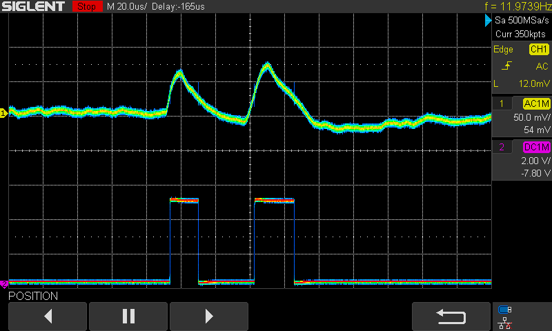
Baseline restorer
Baseline restorer circuit was introduced to reduce impact of DC shift or local baseline oscillation on measured impulse value. Because of the low amplitude at the output of the BLR a bunch of component values had to be altered. The input RC filter values of the block were set to 100nF and 510 Ohms. Then R7 was set to 300 and R8 to 33k to maintain the rule that R7<<R8 so that the output is remains to DC. The load resistor R18 was also changed to 1k. With such values the range of output amplitudes was extended. More information about this intricate circuit can be found here.
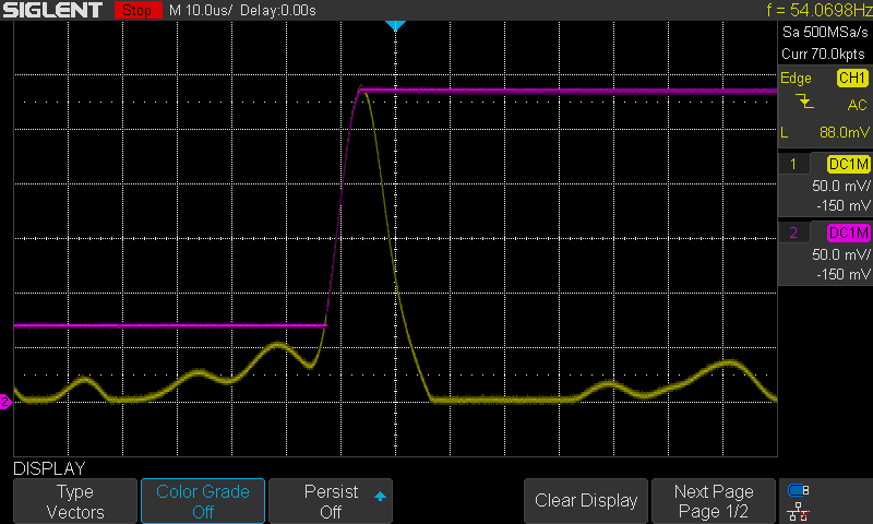
Oscilloscope screens presenting the output of the BLR in comparison to the filter output. The baseline shift cancellation effect is clearly visible.

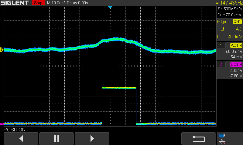
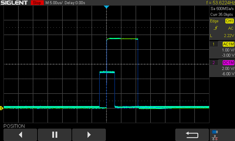
Peak detector
The only block that didn't require any action and worked from the beginning was the peak detector. The sample and hold circuit perform really well as expected. For the tests it was gated with a square wave with frequency about 1-2 kHz.
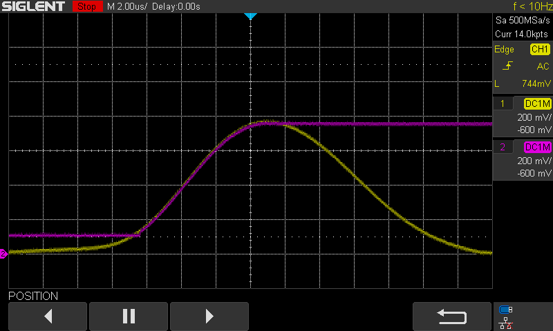
Screens depicting the performance of the S&H in reference to BLR output:
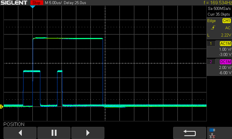
Pulse duration comparator
Parallel to the analogue signal processing a digital detection of the pulses with sufficient amplitude is performed. The fast-filtered signal is inverted using IC4A which may require an additional feedback capacitor of value about 10pF. In my case the AD8066 didn't require it but other fast op-amps may need one to prevent oscillations. Again, the reference voltage and hysteresis of the comparator had to be adjusted. Not only did I had to change the values but also the whole divider had to be arranged in such way that it provided positive voltage. The node previously connected to -5V had to be attached to +5V rail. The one connected to the GND remained intact. The reference voltage from the divider was set to 17mV with R47 = 7 and R48 = 2k Ohms in modified arrangement. Hysteresis was set to 13mV by changing the R53 to 256 Ohms and leaving the R58 with 100k.
Observed behavior showed no signs of double triggering but minimal transient oscillations were noticed in the filter output probably due to crosstalk or connected oscilloscope probes.
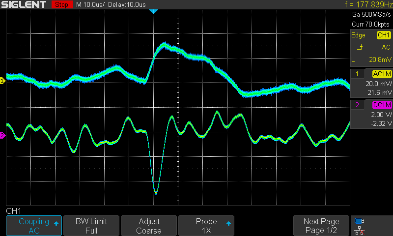
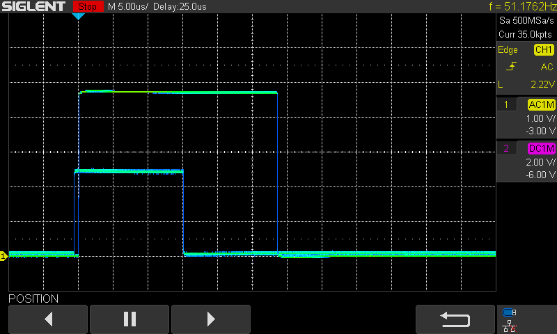
Differentiator amplifier
Additionally, to the pulse duration detection a rising slope detection circuit is implemented using a differentiating op-amp and comparator. To tune the differentiator to required sensitivity the input capacitor was replaced with 1nF and the feedback resistor value was increased to about 660k Ohms. With such values the circuit enables quick signalization of the rising slope with short recovery periods.
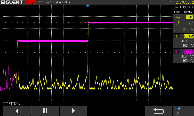
Oscilloscope screens showing differentiator output in regard to inverted fast filtered signal.
Rising slope comparator
After the differentiator amplifier a comparator is located to signal the rising slope by digital state to the MCU. The threshold was adjusted so that only slopes steep enough are detected. R49 = 2,2k R50 =2,9k the hysteresis value remained the same. Performance of the rising slope detector in regard to filter output can be seen on the screens below:
To verify how well the digital detection work, I performed a simple comparison by observing the output signals of the comparators. As can be seen below the pulse duration signal is almost always preceded by a rising slope indicator. I even managed to capture a double trigger of the rising slope signal which indicates possible pile-up, in such case the sample should be rejected and not measured by the MCU.
What's next?
Finally, the preamplifier and signal processing units provide acceptable signals and performance. With that I am able to advance further. The next step is to program the MCU - STM32 to capture the amplitude of the pulses, count them and maybe store them on the SD card. A lot of tests are required to verify if the "blue pill" MCU will meet up the expectations. The whole code structure and functionality needs to be carefully thought over. The core function is to measure the amplitude - energy and count the pulses. Whereas this will be performed in real time through serial port or during period set by user I am not sure. A lot of problems to be solved. It is quite unsettling that only then will I be able to tell if this whole design was worth the effort.
The fourth version should have all the improvements that I mentioned through the log and be just a little bit less flawed.
Discussions
Become a Hackaday.io Member
Create an account to leave a comment. Already have an account? Log In.