 Johannes
I started with the circuit for the LEDs. Soldering them together in parallel, adding a power transistor (or two for left and right side) was all whats needed.
Transistors were used to open the possibility to add PWM to adjust brightness.
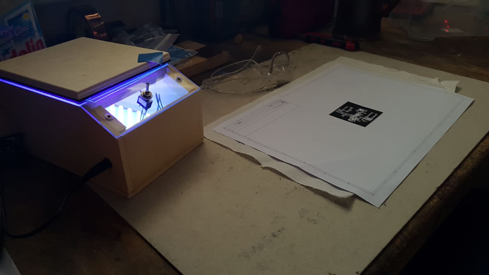
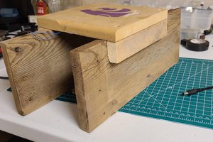
The small wooden box was made out of scrap wood lying around.
PCBs will be placed in a distanve of ca. 50mm to the LEDs. This is a good distance where flow of light is homogenous. Too close and each LED will create a brighter spot, too far and the device will become too big. UV will be absorbed by many materials, I tested some materials and used plastic which did absorb the least amount of light.
Testing was done by shining uv on a sheet of paper and placing materials in the path of light. Good absorbing material results in darker lit paper.
On top of the box is a wooden lid with foamrubber.
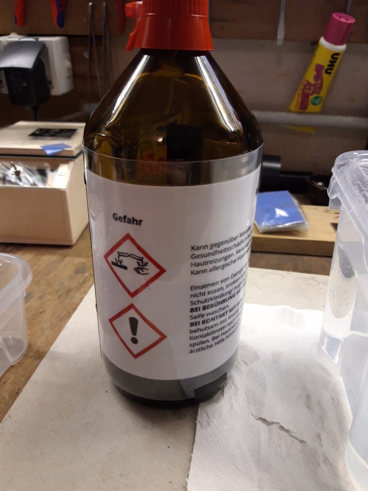
I tested several exposure times, 150s to 180s had the best results. As developer I use NaOH dissolved in water.
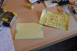
The next time, I make PCBs, I'll take some photos and upload them.
/update/
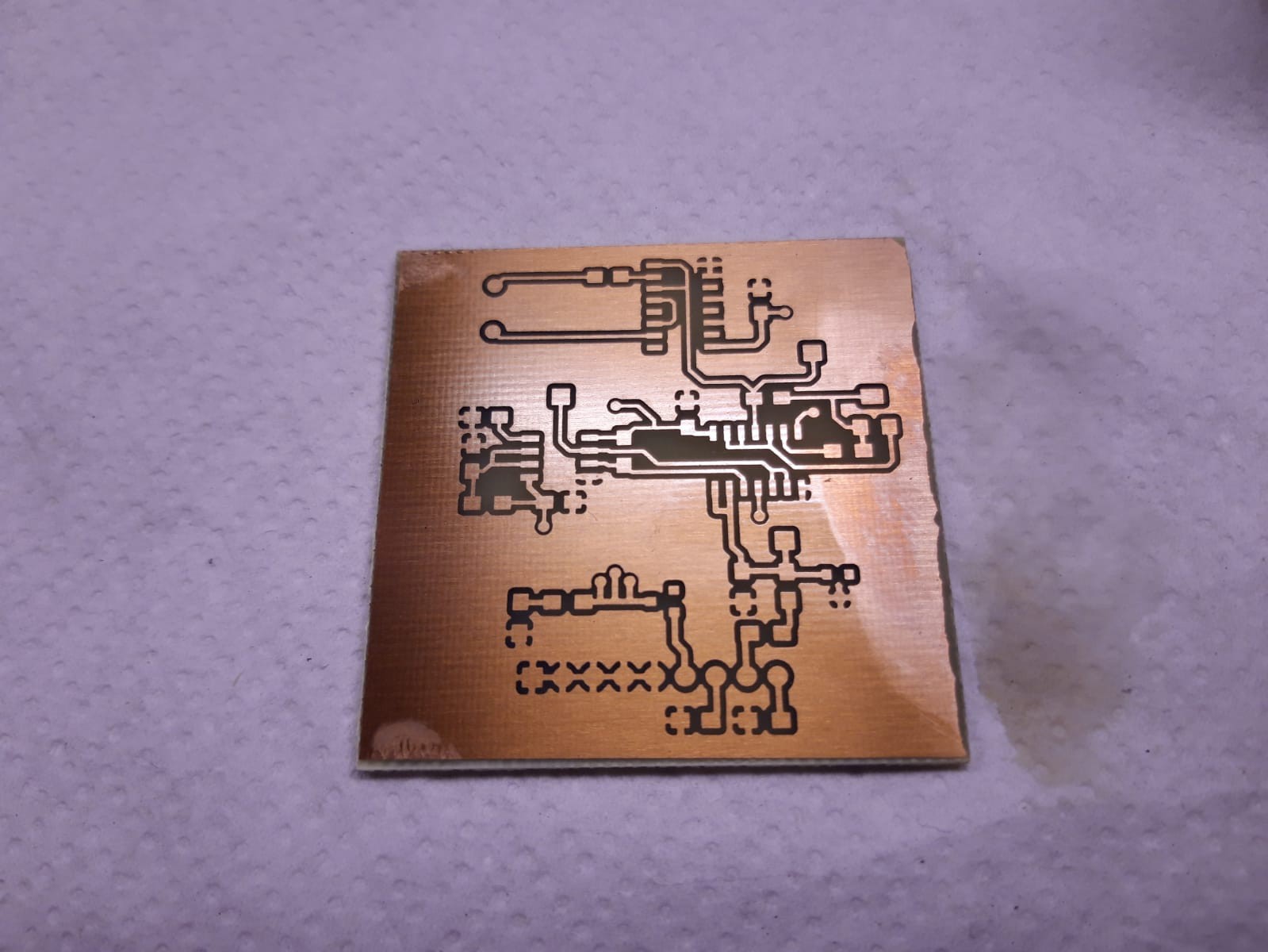
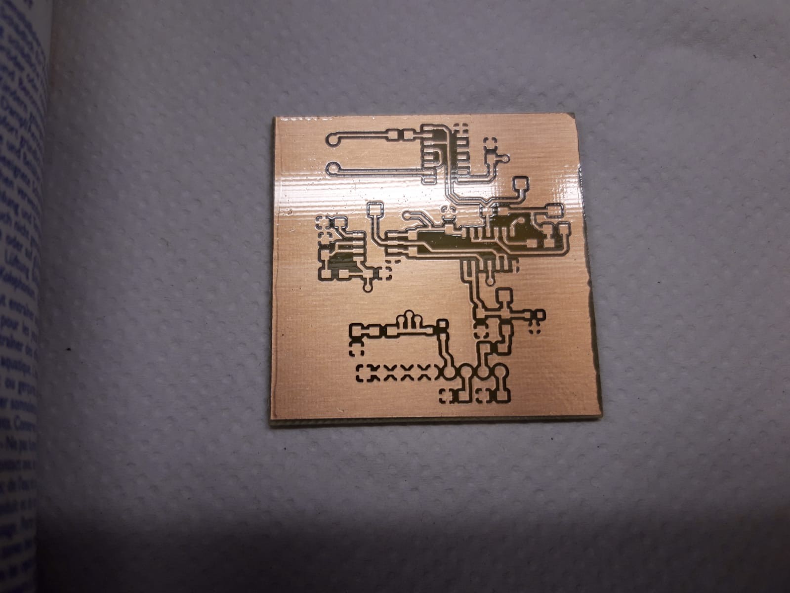
I added two photos showing the first two boards made.
The first board was to test several traces and timing. I learned that 150s is a good time for my boards and foil setup.
With the second board something went wrong, there are some bad spots on the ground plane. I plan to improve this in future boards.
I'll also add details about used chemicals.
 KSUdoubleE
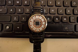
 w_k_fay
 Jeremy Gilbert