 Johannes
I promised to share some details about timing and chemicals.
So far I used the exposure unit three times. At first with mixed results and the third time with quiet good results. Three is not an adequate sample so future results may vary.
Safety first
Whenever you use chemicals be aware of the potential dangers.
I will not go into detail about all dangers encounters while etching PCBs, but you are generally good to wear personal protection equipment, i.e. safety glasses, gloves and tight clothing.
If in doubt, ask someone who may have some experience in the field or don't do it.
Also: Do not store chemicals in bottles used for food or drinks! Pharmacies sell glass bottles for some bucks. Use them!
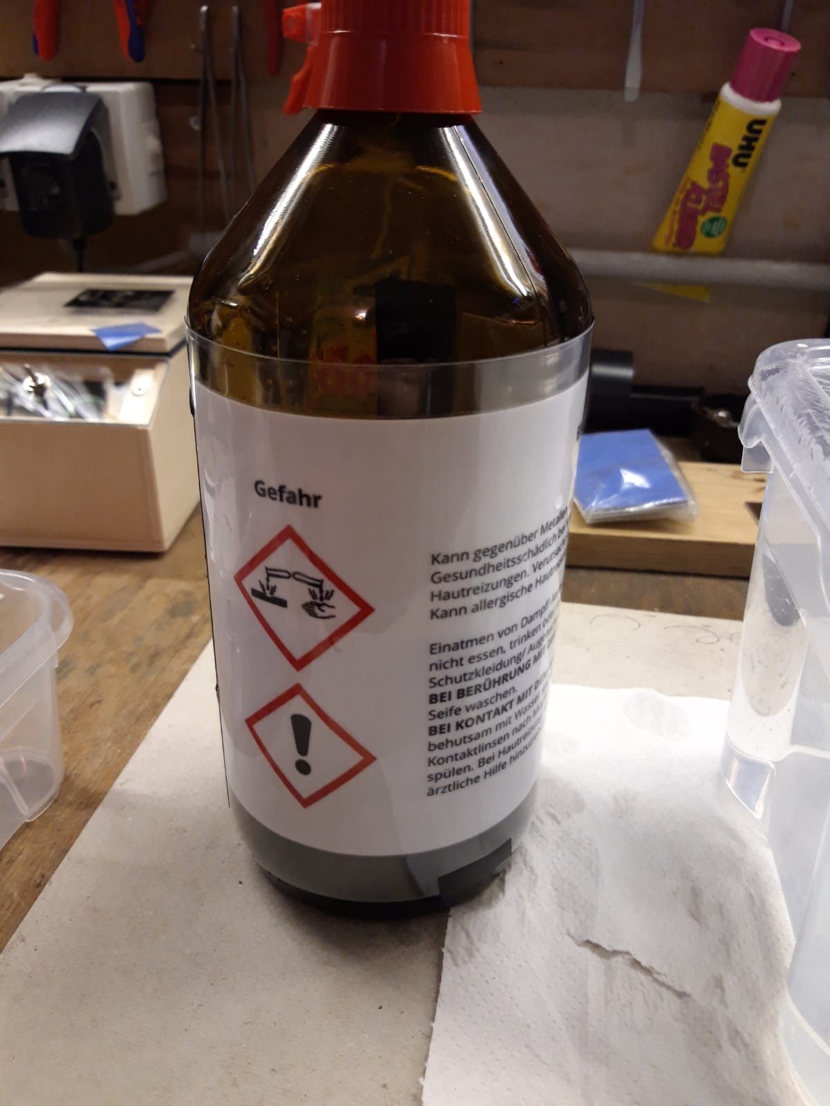
Also label every bottle.
Even if there is only one or two.
Even if you are the only one using them.
You know the difference, someone else may not.
And 'someone else' may be the ambulance who try to rescue you after something (else) has gone wrong.
(Thankfully I do not speak from experience)
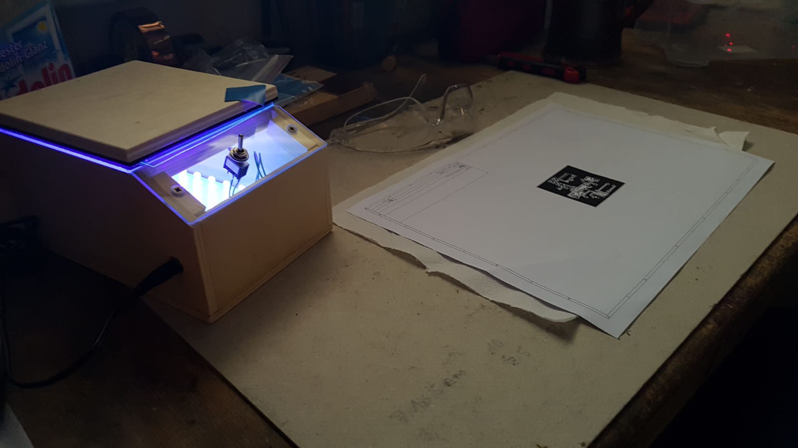
My current setup for PCB etching is:
Exposure
- print out the layout two times on transparent foil, printer setting on 'foil' with a laser printer.
Wipe both foils clean of any dust or particles.
- align them and tape them together. This is important as one sheet will not provide enough 'blackness'.
(I tried toner-density spray on single foils which did not work at all with two different printers.) - Without any bright light present remove protection from the PCB. Place layout on PCB and tape both together.
Place PCB-foil-sandwich in exposure unit and turn on UV light for 2:20 minutes (or 140s).
Developing
- remove everything from PCB. Place it in developer.
Developer is just 10g NaOH dissolved in 1l of distilled water. After some time the traces will be visible.
I let the board in the developer for about 4 minutes (240s) at 20°C. - rinse board with clean water.
store developer in chemical bottle for reuse.
Etching
- Place board in etching solution.
I use Iron(III)chloride. - My trick is to store all chemicals at room temperature. This is easier but FeCl3 works best at higher temperature. Therefore I bought a water bath for the etchant bath, see photo below.
When i put the board in, the etchant had approximately 40°C, the water bath had 60°C.
This way I do not need a hot plate or similar. - constantly move boar in solution. After 6:30 minutes (390s) all traces were clear.
- again: rinse board with clean water, store etchant in chemical bottle for reuse.
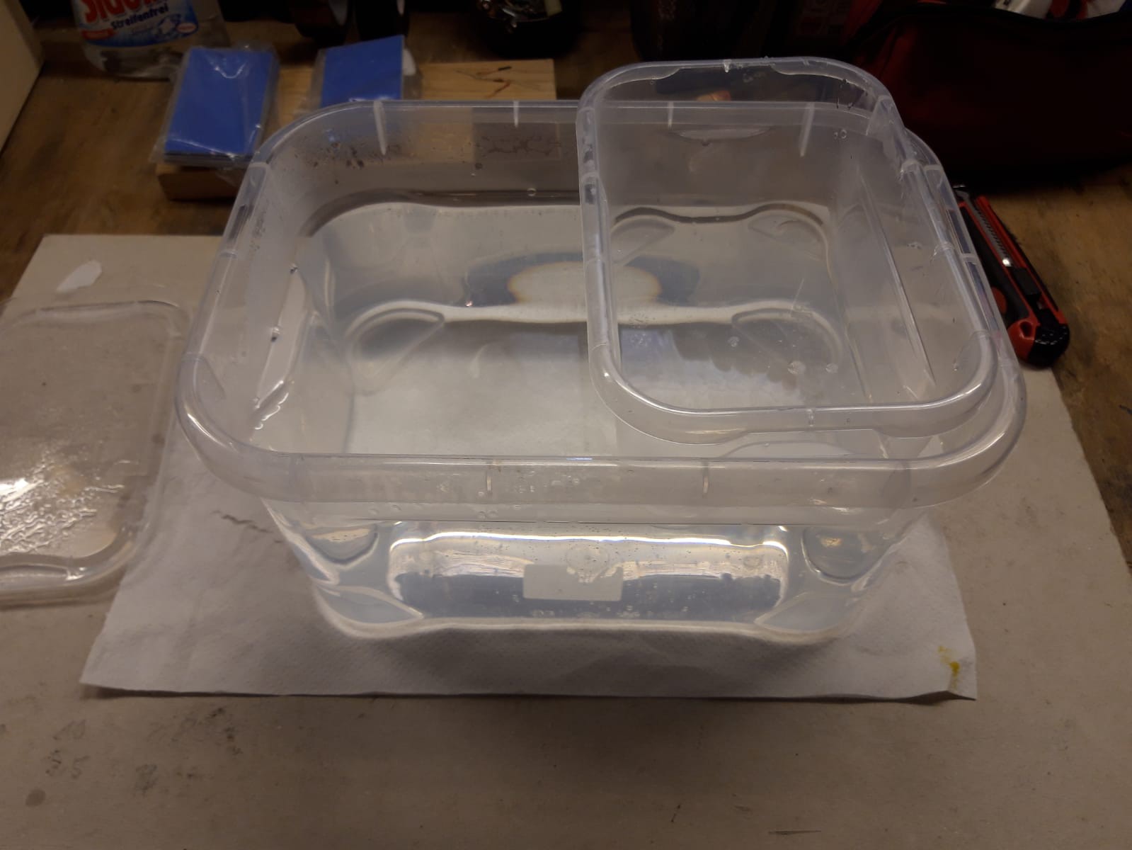
While working on the board, I had no time to take photos. So this is the hot bath without etchant.
After treatment
When you finished the last step above, the board is (theoretically) ready for soldering.
Anyway it is easier, if you remove all photoresist and replace it with solder-varnish.
It is way easier to solder to that, even if it says that the photoresist should be easy to solder - it is not.
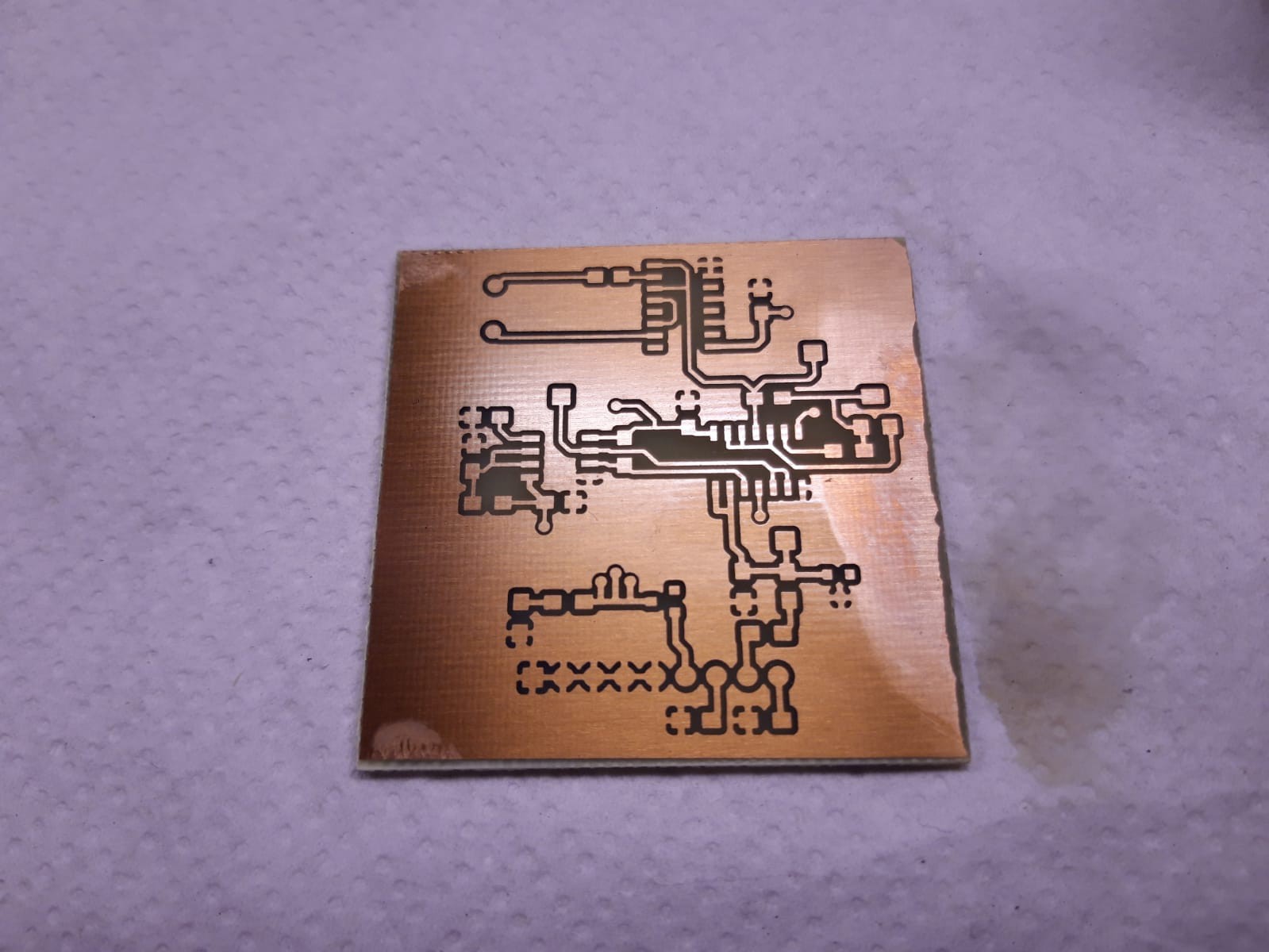
Photoresist is (partially on the right) removed with alcohol or acetone.
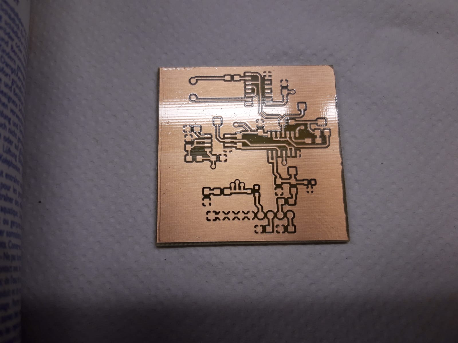
And this is the board with solder-varnish.
Discussions
Become a Hackaday.io Member
Create an account to leave a comment. Already have an account? Log In.