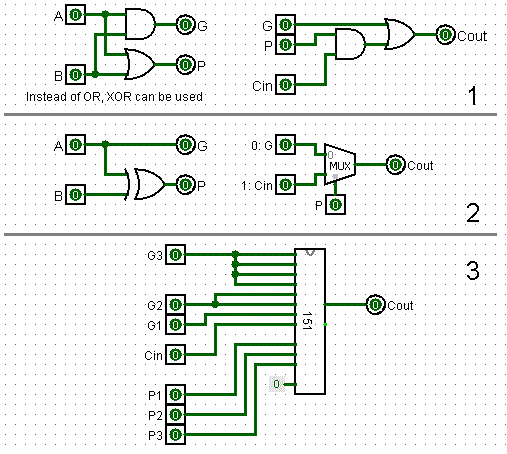
The first diagram is the classic carry circuit. The left side uses the two inputs A and B to generate P (propagate) and G (generate) signals. The right side shows how P and G, together with the carry input, produce the carry output signal.
In the first diagram, when G=1, the P output is actually a don't care. But for our solution, P must exactly represent if the input carry must be propagated to the output. We can do that by generating P with an exclusive-or (2nd diagram). Now, when P is active, we activate a switch (the mux) to connect the output carry to the input.
What to do when P is not active ? If P is not active, there are only two input situations:
1) A=0 and B=0 2) A=1 and B=1.
Only in the 2nd case, a carry must be produced. So, we can simply connect the second multiplexer input to A (or to B, since A and B are the same when P=0).
In the third diagram, the multiplexers of three adjacent bits are combined into a single 74HC151 8-input multiplexer. So for 3 adjacent bits, the Cin has to pass only a single IC before arriving at Cout. Note that the 151 has an enable input, that can be used to disable the carry for the logic functions of the ALU.
And as an extra bonus, since the P signals are "A exor B", they are exactly the same as the signal that is used to produce the sum (the RED wire in the diagram on the previous log). So, the generation of both P and G actually comes totally for free !
[ edit oct 2023: re-inserted the picture that disappeared ]
Discussions
Become a Hackaday.io Member
Create an account to leave a comment. Already have an account? Log In.