 Pavel
PavelFor some time, hardware soldering was put on hold as some different venues, like microscopy, took my attention. But recently, I returned to think about this CPU more globally, and more particularly about memory access operations. This is important, as after finishing the Register File, connecting it to the ALU and a couple of other boards to make a pilot machine, the time will come for actual building of pretty sophisticated memory access circuitry. And this needs some planning, as the way such circuit implemented in the model right now is pretty messy -- I was building it incrementally adding parts and functions to the model on the go.
Following are my thoughts and designing of this subsystem using more top-down approach, which yielded very clear and quite simple solution:
2021-06-10 ... 14
Updated register model
While thinking about addressing circuitry, and how to reconcile all of the different register sizes (8 bit for Hi8 and SR and IO ports, 16 bit for GPR and 24 bits for address pointers), it occurred to me that there is a better approach -- that I should get rid of all these different sizes and go with one size -- all addressable registers are to be 16 bits wide.
In the new config following registers are included:
- 16 addressable registers:
- 8 General Purpose Registers: the 16-bit registers which are connected to main ALU, and which are used for data manipulation;
- 8 Memory Pointer Registers: the 16-bit registers used in pairs to form 32-bit memory addresses (Program Counter, Stack Pointer, Frame Pointer and Base Pointer), connected to 32-bit Address Adder;
- 1 visible(?) special register:
- Status Register, a collection of latches used for holding machine state (Carry, Overflow, Negative, Zero, and Interrupt masks, and possibly other info(TBD)), connected to Data Bus as 16-bit value;
- 2 invisible (background) registers:
-- Instruction Register (16-bit): holds currently executing instruction;
-- Memory Address Buffer (32-bit): additional memory pointer, used in some of the addressing modes.
- ??? may be some other registers which I do not know about the need of.
In the above model there is no dedicated Input and Output registers inside the CPU -- all I/O would be memory mapped.
On the other hand, there is now plenty of addresses for all the needs -- actually 4Gig of them. The machine still will have max 16MB of actual installed memory, mainly due to cost considerations, but making virtual memory will be simpler.
For this much addresses the adder will be bigger and more complicated than in the main ALU, due to it being 32-bit, and for it to not be bottleneck for speed, it probably should have 2-stage carry-look-ahead unit.
Each of the 16 addressable registers can be loaded and stored to memory. Special instructions may do the same for SR, but with some restrictions (most probably this should be done at function call and interrupt servicing sequences).
The Memory Pointer registers are to be loaded and stored in pairs, as 32-bit values.
Probable extension to loads/stores of several words in one instruction. This will be 1, 2, 4 or 8 words, (may be even 16 words, but there are doubts about this).
Also there needs to be provision for loading/storing individual bytes, will make work with characters and strings easier.
Following modes are desired:
0: Immediate load (2-word instruction):
Loading the word right after instruction into a register. There is no corresponding store, as it not useful.
Uses: pre-loading registers with initial data values;
Modified version is a step in direct memory access, when address is encoded into instruction
2 variants: load 16 bits of data, and load 25 (or 24) bits of address
1: Direct loads and stores at address encoded in instruction (2-word instruction):
Thus address ranges 0x00000000-0x00FFFFFF and 0xFF000000-0xFFFFFFFF are accessible.
(Accessible address ranges would be 0x00000000-0x007FFFFF and 0xFF800000-0xFFFFFFFF if 24 bits of address could be loaded.)
Bottom part is reserved to RAM, while top part is for ROM and I/O.
2: Loads and stores at address in Memory Pointer, with offset of up to +-32767 bytes (1-word or 2-word instruction):
Full 4Gb of address space is accessible, Virtual Memory need to be implemented for full use.
This is the mode for regular memory accesses.
3: Loads and stores at address in Memory Pointer, with post-increment/decrement (1-word or 2-word instruction):
Data is accessed at address in Memory Pointer, same as (2) and the Memory Pointer value is updated.
To be used in loops and stack operations, also for simple memory access without offset when post-increment value is selected to be 0.
This is the mode for regular memory accesses, more restricted but faster than one with offset.
4: Loads and stores at address in Memory Pointer, with pre-increment (1-word or 2-word instruction):
Value in the memory pointer is updated, and data is accessed at new address.
To be used in loops and stack operations.
Offset value sources:
+0 - hardcoded -- default;
+2 - hardcoded -- used for incrementing PC, and popping words from stack;
-2 - hardcoded -- used for pushing words to stack;
+Data16bit(signed) -- data placed to bus, can come from one of GPR, or from memory, most flexible way of data access;
Possible extensions:
6: indirect access (by reference in memory, the pointer variable) -- probably can be done using combination of the above modes.
2021-06-15
Register transfer scheme for the CPU
I've finished graphical representation of register transfer model, and it looks neat:
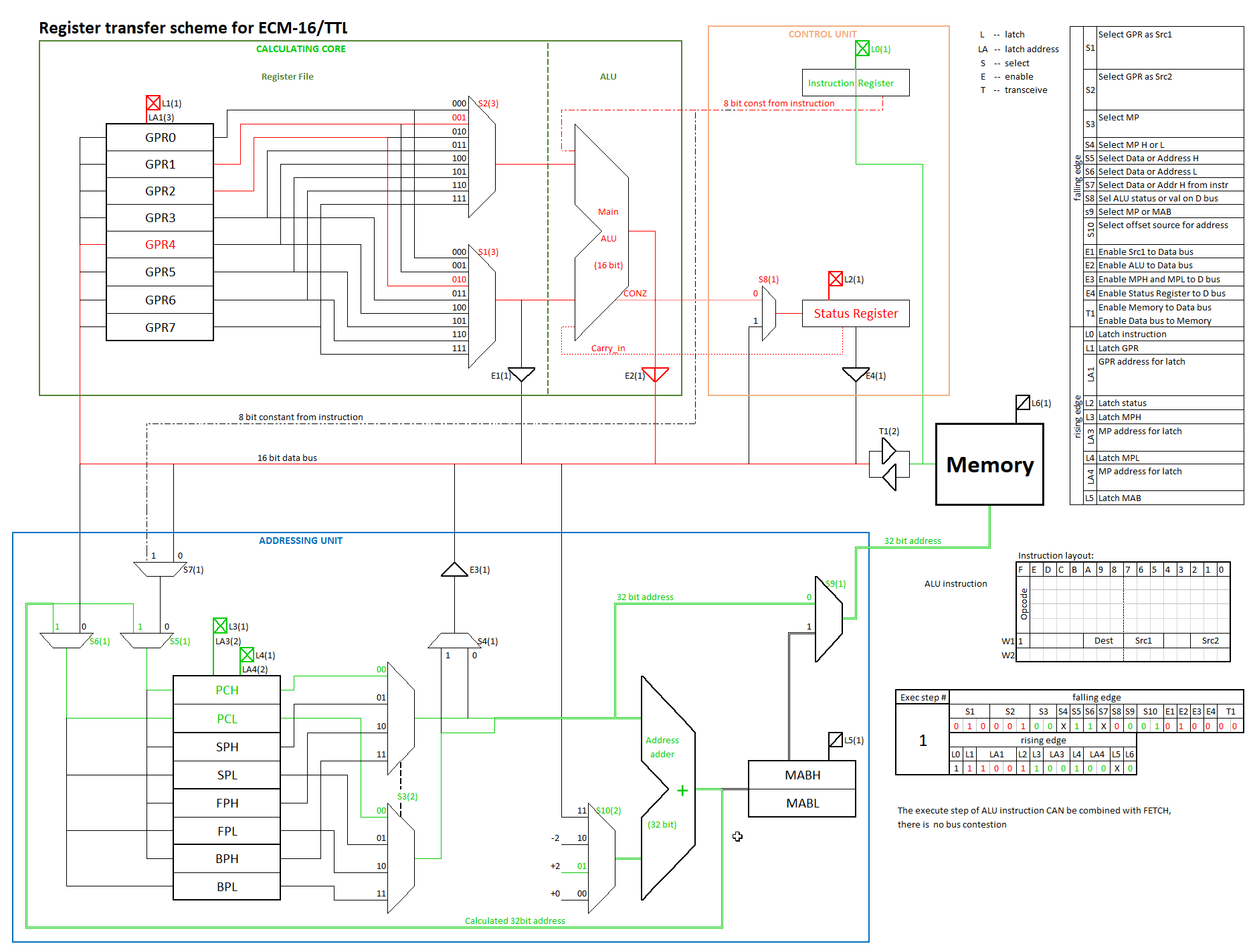
Above picture shows all planned registers with data paths connecting them.
It also shows an example of designing of micro-instructions, in this case an ALU operation, combined with fetching of the next instruction. As, per this model, there is no congestion over any bus, these two steps can be done in one clock cycle, and thus, when there are many such instructions in sequence, they are essentially executed one instruction per clock cycle.
I now wonder why I haven't done this earlier, as it would have clarified so many aspects of my CPU.
This representation will also greatly help in designing micro-instruction sequences for CPU instruction set, specifically ones involved in memory accesses.
Regarding these instructions, I am confronted with scarcity of instruction word bits for assignment of instructions, and therefore part of what I want cannot be implemented because of this. Time for tough choices had come.
It is unclear to me if I really need instructions for accessing single bytes of memory. There is a strong perception that unpacking/packing bytes into 16-bit words using main ALU will not be much slower than fetching and storing those bytes to memory one by one. And ALU operations are fastest of all, they are going to be executed effectively at 1 instruction per 1 clock cycle, when in sequence.
Another thing is loading/storing multiple words per instruction: this would be very nice thing to have, as it would make some loads/stores faster, but they are not necessary for CPU to work properly.
2021-06-16
Thoughts regarding circumventing instruction word's "bit scarcity"
One possible solution regarding bit scarcity just occurred to me. What about using some sort of presettable flags to modify base instruction? Like having BYTE flag, that if set makes all memory accesses 1-byte? This, and other possible flags for other purposes will fit into Status Register, so no new places to store this information will be needed. It will introduce delays, and one should always be careful to clear it right after need is removed to avoid problems, but it looks like a viable solution. It looks like some kind of "prefix", as it will most frequently used right before memory access instruction (like, 1: SETBYTE; 2: LOAD to RegX from AddrY).
Discussions
Become a Hackaday.io Member
Create an account to leave a comment. Already have an account? Log In.