 Pavel
PavelFirst, semi-experimental board with fast adders was completed at spring of 2020. It had a number of defects, and at the time I ran out of solder and as I was waiting for new batch to arrive from China, somehow I've lost interest in the project, so it was lying around just like that. This year, after some time playing with spectrometer project, I thought maybe revive this one, and took a hard look at the board, and debugged it; now it seems to be working good.
The defects were all due to the bad soldering, the wiring itself was fine. In several points solder joints were bad, as solder didn't made contact as needed. Also at some points these solder points broke after some time being okay, as the board itself was quite flexible, and the flexing of it led to joint breakage. To mitigate this in future, I glued plastic strips to the board to make it stiffer.
The board has mostly the same input/output interfaces as the 8-bit ripple adder made of discrete components (using diode-transistor logic), the control panel from that project is perfectly useful for testing this new one made of 74HCXX chips.
After successful debugging, I compared the speed of the new circuit to the old one, and results are quite fascinating:
The adders were setup to make the addition of carry_in to operands summing up to 0xFF, i.e.: 0x00 + 0xFF + C_in => C_out (0x1) + 0x00.
The carry in signal was fed from rectangular signal generator, which was also used as strobe signal for oscilloscope, and the carry out signal was measured by the same oscilloscope, thus the delay was measured.
For the DTL 8-bit ripple adder, the delay was near 30 microseconds, while for a pair of 4-bit fast adders with carry look-ahead, made of CMOS chips, the delay measured was tiny 120 nanoseconds, or almost 300 times less! Of course, this comparison is more like apples to oranges, but nevertheless, distinction between these two technologies is made very obvious by it.
Following are some photos of board building and testing:
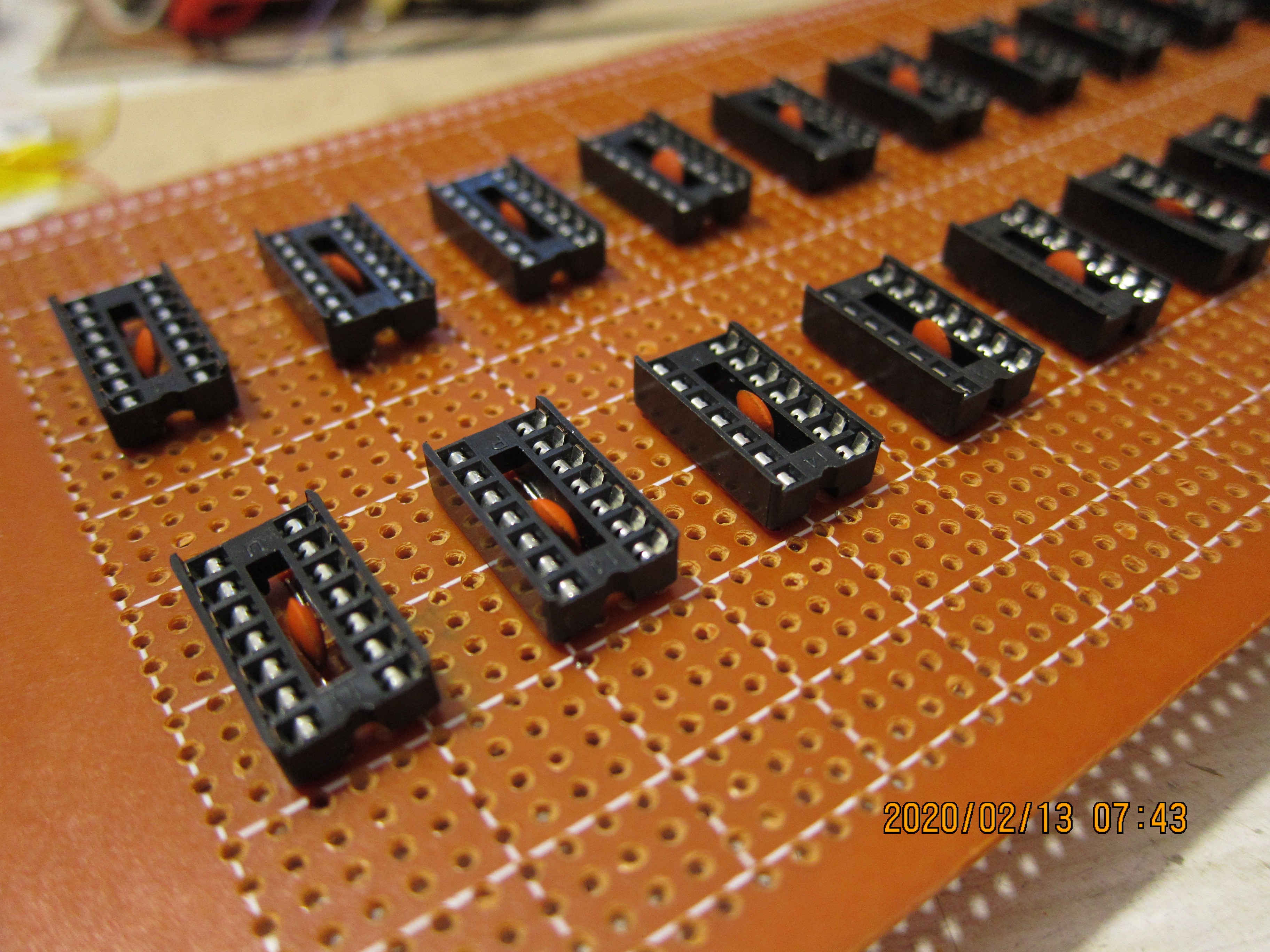
1.1. basic layout (IC sockets only) - top:
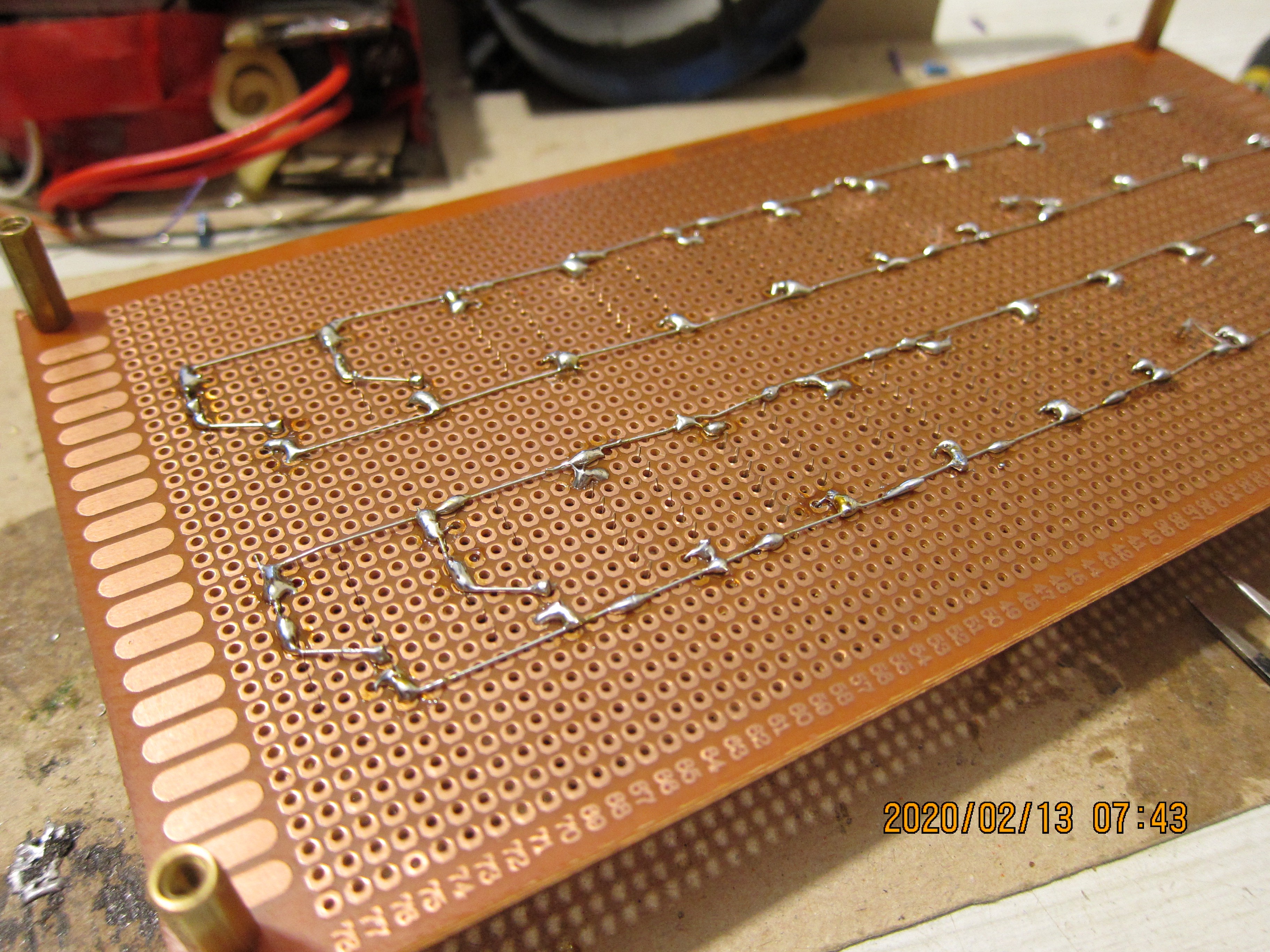
1.2. basic layout - bottom:
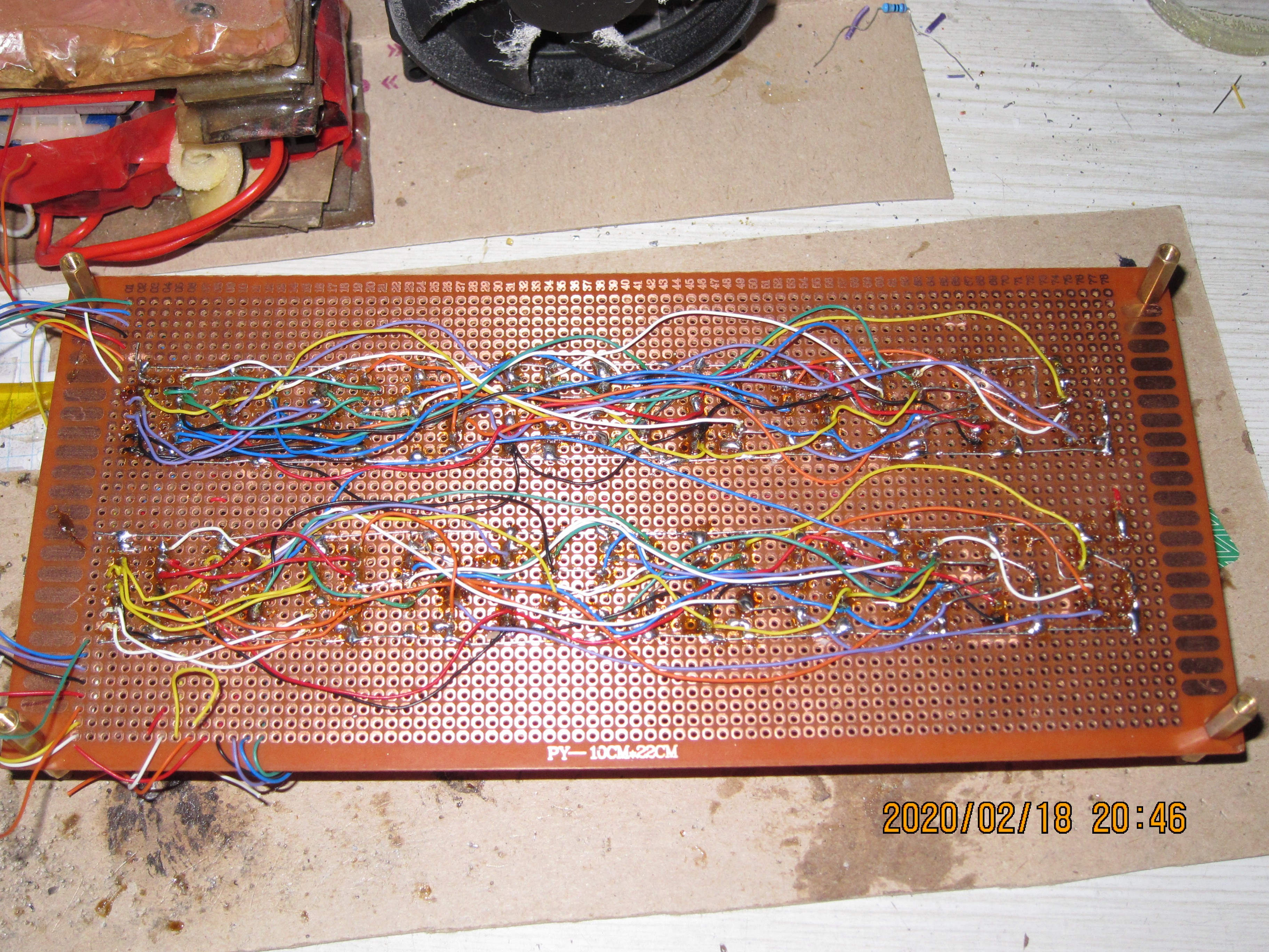
2. Connecting the IC sockets in a way that makes the board a functional fast adder once proper chips are inserted into them:
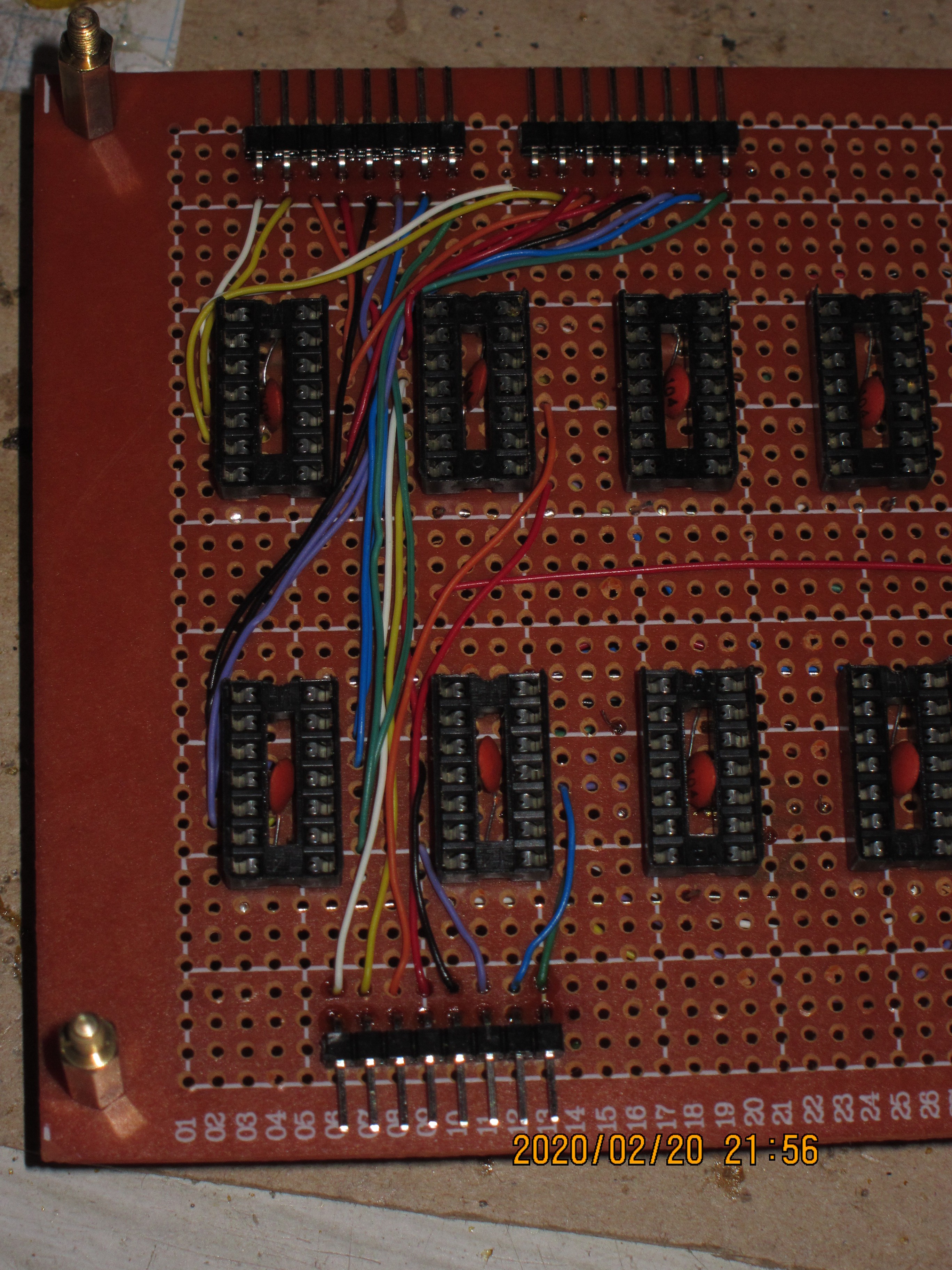
3. Making the input-output interface for the board:
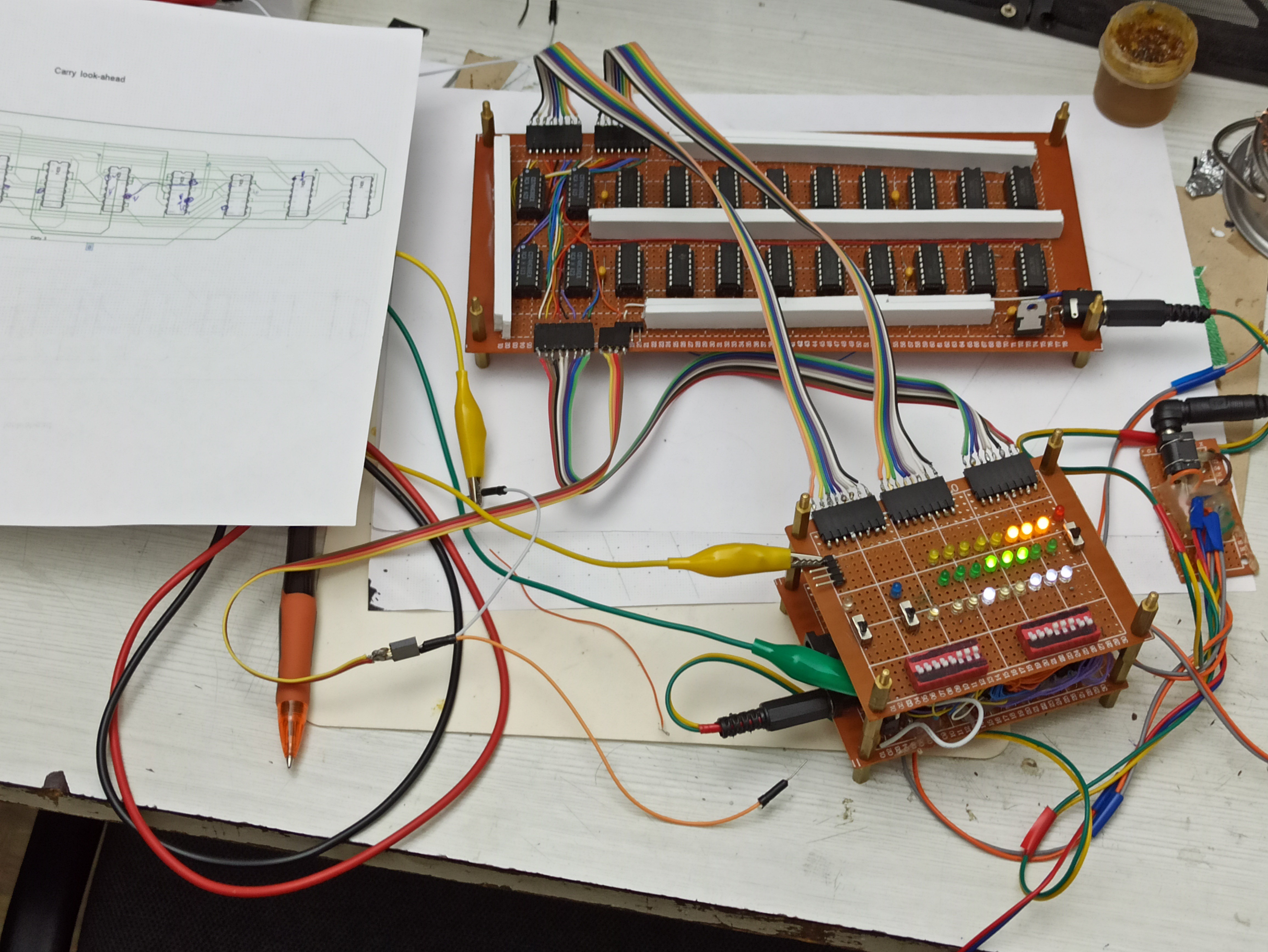
4. Testing the board using control panel from DTL adder project:
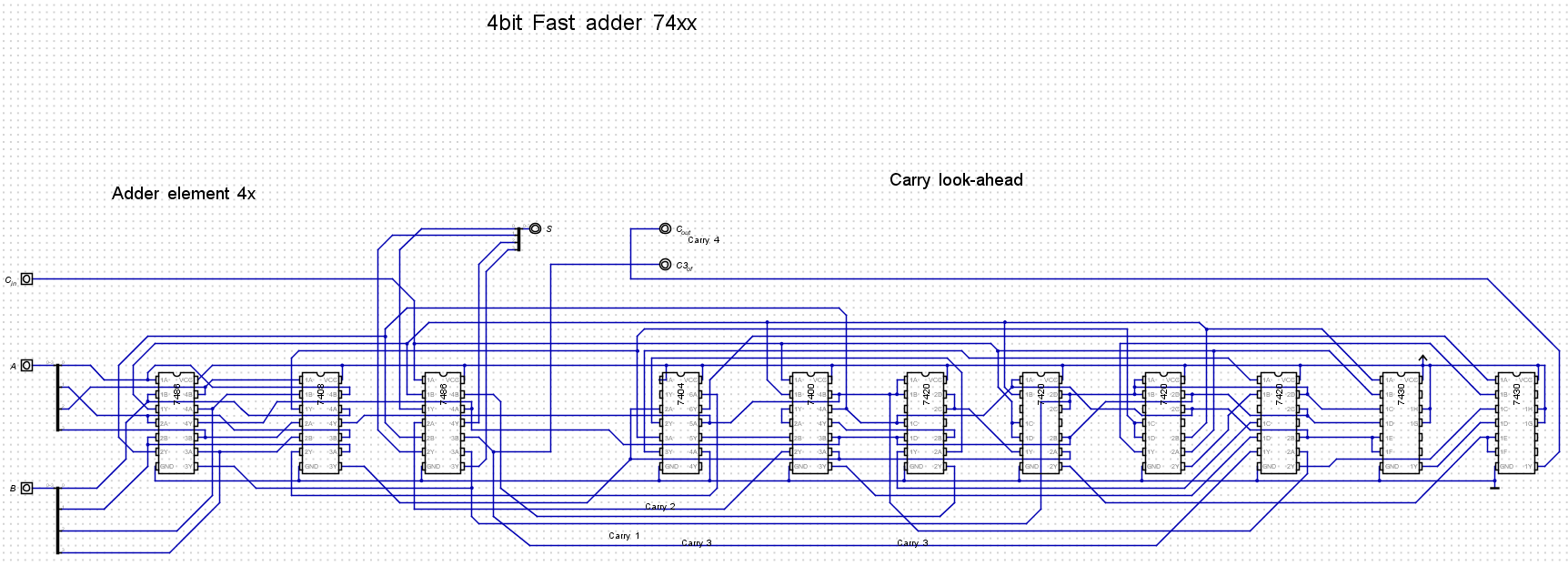
5. Schematic of the 4-bit fast adder, using chips, and optimised for minimum wire clutter and to be close to the way it is done on real board (the board itself holds two of these):
6. Schematics of parts of above circuit, done with individual gate symbols:
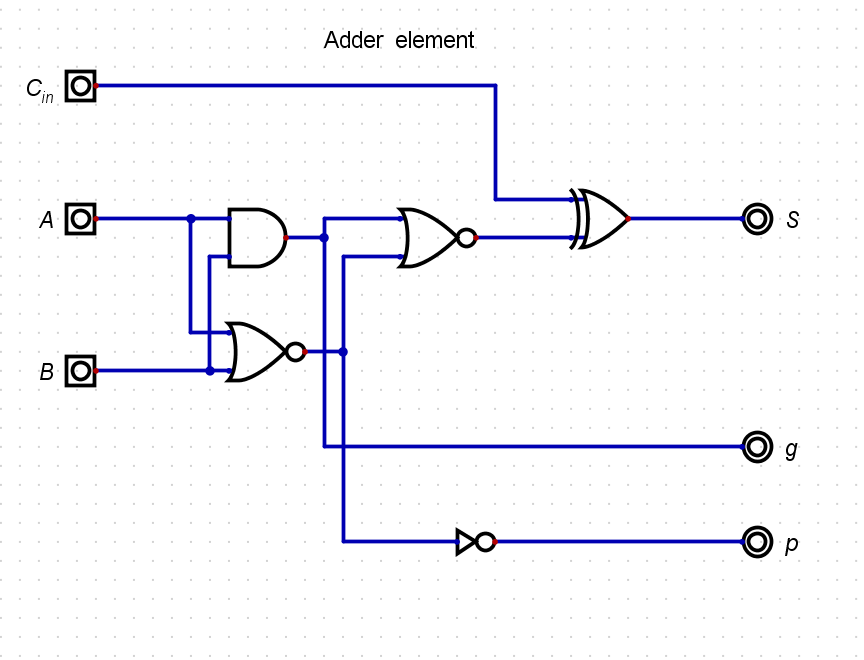
6.1. 1-bit Adder elements (4 of which are made with 4 leftmost ICs on the schematic above):
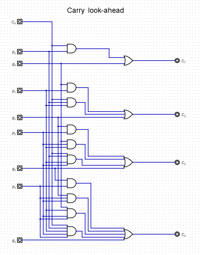
6.2. Carry look-ahead for 4-bit adder:
Discussions
Become a Hackaday.io Member
Create an account to leave a comment. Already have an account? Log In.