We’ve been making a lot of exciting progress towards the completion of the wearable prototype design. The wearable prototype schematics have been finalized at revision 1.1, which has been uploaded. The only major change in this revision is the removal of the potentiometers used for control, as the GUI has advanced to the point where they have been deprecated.
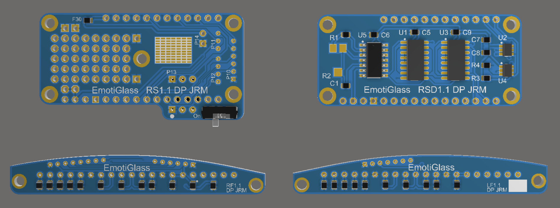
The wearable prototype breaks the circuitry into 4 small PCBs:
The right side pcb mounts to the frame and provides a termination point for all of the wiring going to the other boards and to the components which don’t mount directly to a PCB (side shutters and battery). The feather plugs into this board, which contains a fuse on the battery input and a soft power switch. It also contains a socket for the pulse sensor to plug into, which was intentionally selected and oriented so that it will easily disconnect if the wire is accidentally pulled. The shape of this board was driven by the feather, so there was extra space which was filled with prototyping area to facilitate rework or feature addition in the future.
The right front and left front PCBs contain the capacitors needed for operating the LCD displays. The right side also contains the light sensor for the auto darkening function.
The right side dev PCB contains the hardware LCD drivers. These will be replaced by firmware, eventually, which is why they are on a separate PCB. This PCB will stack on top of the feather.
Layout of these 4 PCBs has been completed, and they have been submitted to OSH Park for manufacturing. The gerber zips and a draft of a pdf with layout prints and assembly annotations have been uploaded (this will be updated after we assemble our initial batch). We’ve selected the largest surface mount packages available for ICs (mostly SOIC’s) and are using 0603 passives (with plenty of space between them) so that the boards will be reasonable to assemble with only a basic soldering iron.
The boards are designed to be directly wired to each other. A number of interconnect options were considered, but this ended up being the simplest and lowest profile option. While it will be time consuming to assemble, this is acceptable for a few prototypes. 30 awg wire wrap wire will be used for most signals. Wire with Kynar or Teflon insulation is highly recommended. Power and ground will use something slightly larger, probably 26 awg. A draft of the wiring diagram has been uploaded (this will be updated with any changes we make during initial assembly).
Lastly, a draft BOM which contains only the electronic components has been uploaded. This will be updated to include the mechanical components shortly.
Discussions
Become a Hackaday.io Member
Create an account to leave a comment. Already have an account? Log In.