So far we learned a few things about Verilog and how to create a module in Verilog and run a simulation. While simulation can tell us a lot of things about the correctness of our module, there is nothing like putting it on a piece of hardware and seeing it working. In this part of the tutorial, we will walk you through the steps for synthesizing the module and implementing it on Mimas V2 Spartan 6 FPGA Development Board (or Elbert V2 Spartan 3A FPGA Development Board) hardware.
As mentioned in part 3 of this tutorial, the test bench code is used only for simulation. To synthesize our module, we have to remove the test bench code. For those who don’t know, HDL Synthesis is the step where the HDL ( Verilog/VHDL or any other HDL for that matter) is interpreted and an equivalent hardware topology is generated. This hardware topology will be very specific to the target FPGA selected. Synthesis is a very complex process and we don’t need to know the internals to get our simple module up running.
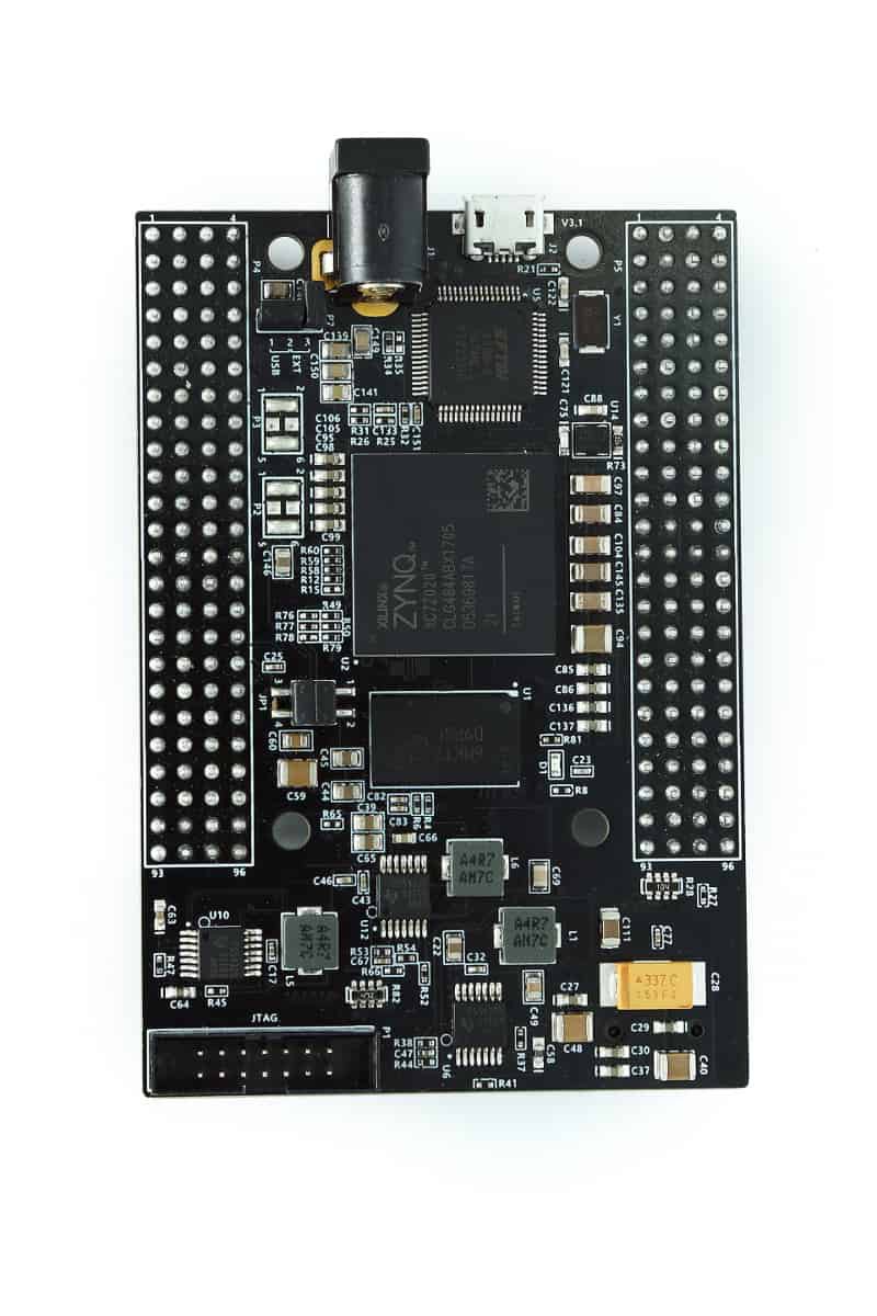
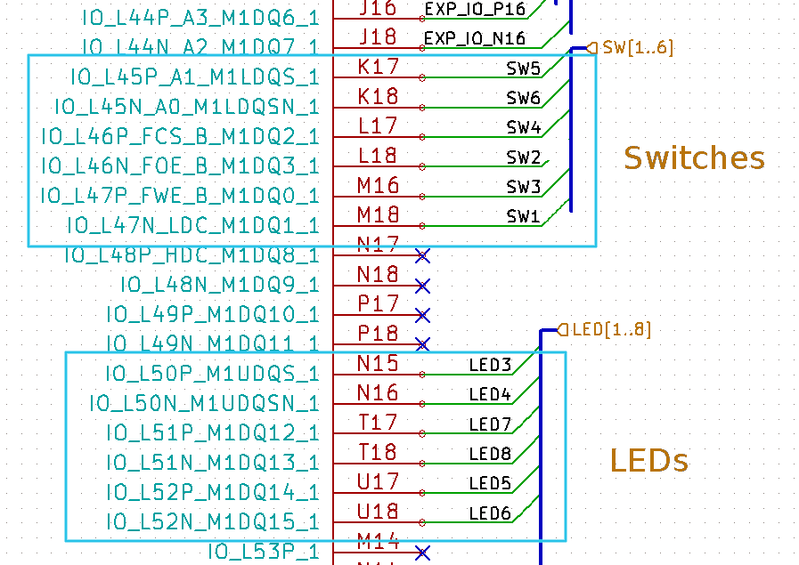
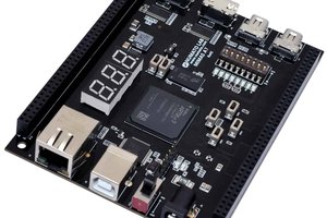
We will use Mimas V2 Spartan 6 FPGA Development Board to implement our module and the steps are very similar for Elbert V2 Spartan 3A FPGA Development Board as well. Mimas V2 board has a Xilinx Spartan 6 FPGA, a DDR SDRAM and a few other peripherals on board. The exact FPGA part number used on this board is XC6SLX9-CSG324. This is a 324 pin CSG324 BGA chip with 9K logic cells. The image below shows the part of the schematics where FPGA IOs for LEDs and Push Button Switches are connected. We will use one Push Button Switch and one LED to implement our logic.
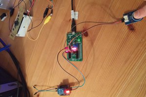
Let’s come back to our module and think about how we can implement the same on the hardware. The module in question is a NOT gate. As we know, the output of a NOT gate is always the negation of the input. We can have many possible hardware configurations to test this module. The easiest would be with a switch and a LED. See the proposed hardware configuration in the picture below.
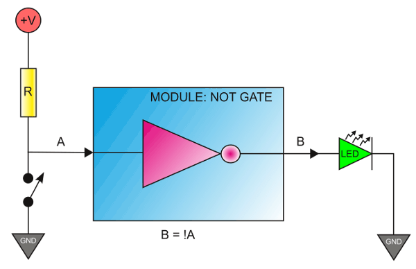
In the above diagram, a switch is connected to an input which is pulled up to VCC using a resistor. The output is connected to a LED. Let’s take a moment to understand how this circuit is going to behave. When the switch is in open position, there will be a positive voltage ie; a logic 1 at the input (A) of the NOT gate. That means the output (B) will be at logic 0. So the LED will be in OFF condition. When the switch is closed, the input of NOT gate will become logic 0 and the output will switch to logic 1 state. And the LED will glow.
Now we know the basic hardware requirements. We need the following in our prospective hardware.
- An input capable IO with a pull-up resistor and a switch attached.
- An output capable IO with an LED attached.
Let’s take a closer look at the Mimas V2 Spartan 6 FPGA Development Board. The following image shows the LED and switch we are planning to use on Mimas V2. Elbert V2 also has onboard switches and LEDs that can be used for this purpose. If you are using Elbert V2, LED8 and Switch SW5 would be good choices (The project attached at the tutorial for Elbert V2 uses SW5 and LED8).
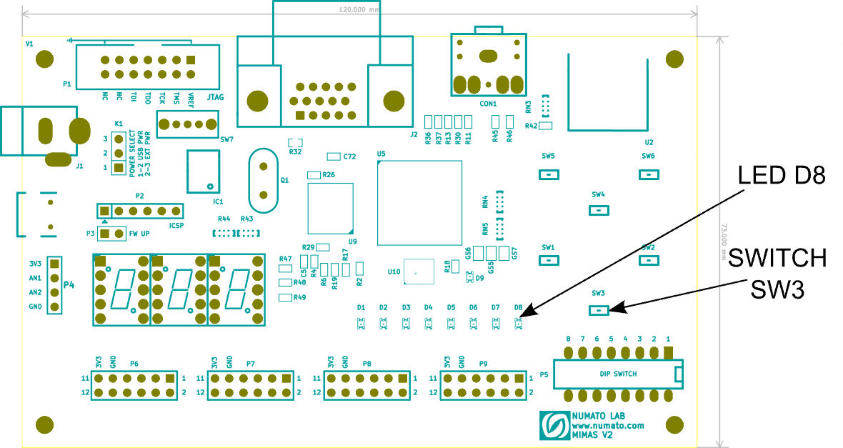
As we see in the image above, Mimas V2 has six general purpose push button switches and eight LEDs for the user’s convenience. We can now take a look at the Mimas V2 schematics and learn a little bit more about where the switches and LEDs are connected. Let’s choose push button switch SW3 and LED8 for our purpose. Looking through the schematics reveals that SW3 is connected to IO M16 and LED8 is connected to T18 of the FPGA respectively (M16 and T18 are not the IO names, rather they are the names of the BGA balls that the IOs are connected to.).
We now have a Verilog module that we want to implement and we have selected a hardware platform and decided what IOs to use for implementation. Let us revisit our module. I’m reposting the module code here.
module myModule(A, B); input wire A; output wire B; assign...Read more »
 Int-Mosfet
 Hexabitz
 Emilio P.G. Ficara