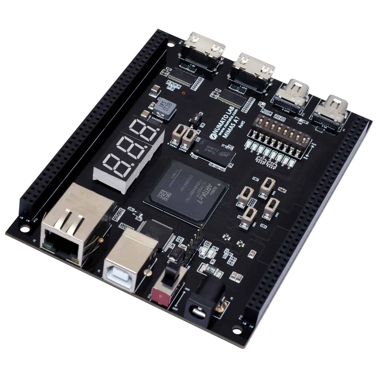
Mimas A7 - Artix 7 FPGA Development Board
Availability of sufficient data storage is a very important factor when selecting an FPGA development board. Various boards offer different memory options such as SRAM, QDR, SDRAM, FLASH etc. DDR SDRAM is most popular of all since it offers a reasonably large amount of volatile storage that can be accessed at a reasonable speed. An onboard volatile memory is key for a lot of applications such as image processing, data logging etc. since the Block RAM available in the FPGA logic fabric is very limited.
This article does not intend to visit the basics and architecture of SDRAM rather focus on how to create a very small project to show how to work with DDR SDRAM connected to an FPGA, specifically Xilinx Spartan 6. There are a lot of informative articles on the internet where a curious reader can learn about the inner workings of SDRAM. We found this tutorial series very informative. Please note though that a deep understanding of the theory behind how SDRAM works is not necessary to follow this tutorial.
We will be using Numato Lab’s Mimas V2 FPGA Development Board for this tutorial. But these steps can be applied to most other boards with minimal changes.
To make SDRAM work with an FPGA, we will need a few essential components.
- Memory Controller
- Wrapper logic
- User logic
Memory controller is the component that talks to the DRAM directly. This component generates the necessary signals (Address/Data/Control) to establish communication with the memory. Memory controller can be implemented in code or could be an IP block built into the silicon. Some FPGAs may not have a physical memory controller inside and the only way to interface DDR is to write code manually that uses FPGA logic resources. This takes up valuable space in FPGA logic that could otherwise be used for other purposes and also performance is usually not as good compared to hard IP memory controllers. A large number of FPGAs do have built-in hard IP memory controllers. Usually, these FPGAs are more expensive but built-in memory controller offers better throughput and less FPGA logic usage.
In most cases where memory controllers are available on silicon, the interface may not be readily usable by the user’s logic. In such cases, it is necessary to have a wrapper code that can interface with the memory controller core on one end and present a simple and consistent interface to the user logic. Usually, wrappers offer an interface consists of a number of ports that can be read/written by the user logic.
User logic is the final piece of the puzzle. The user code is the piece that generates, consume data. While working with the data, user logic may store the data temporarily on SDRAM (or any other memory device for that matter). For example, a data logging application running in FPGA may acquire samples from an ADC, store it in SDRAM. This data will be read back from the SDRAM and sent to a PC at a later time.
It may seem very complicated to get all this done. But don’t worry, there are tools that can help. Xilinx has done an excellent job of creating some nice tools that can help us generate all the above components and get our test application running with minimal or no manual coding. So you can forget about the stuff above for now, but this bit of knowledge is useful later when you are planning to use Memory Controller in a real-world project.
Let’s take a quick look at the board that we are going to use. Mimas V2 has a Xilinx Spartan 6 LX9 FPGA in CSG324 package (has two built-in memory controllers) and a 512Mbit LPDDR SDRAM ( LP stands for Low Power and DDR stands for Double Data Rate). The FPGA’s CSG324 package is important here because Xilinx Spartan 6 LX9 is available in some other packages that don’t have a built-in memory controller. Of the two memory controllers available on the FPGA, one is connected to the 512Mbit LPDDR SDRAM and the other is left unused. All connections and other...
Read more »
 jlbrian7
 Mike Lemberger
 f4hdk
f4hdk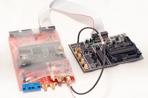
 Colin O'Flynn